Manufacturing method of display device and display device

a display device and manufacturing method technology, applied in the manufacture of electrode systems, electric discharge tubes/lamps, discharge tubes luminescnet screens, etc., can solve the problems of color unevenness, uneven brightness, and difficulty in completely uniformly keeping the temperature distribution of growth substrates, and achieve excellent display quality.

Active Publication Date: 2010-10-14
SONY CORP
View PDF2 Cites 77 Cited by
  • Summary
  • Abstract
  • Description
  • Claims
  • Application Information

AI Technical Summary

Benefits of technology

[0011]Thus, it is desirable to provide a manufacturing method of a display device in which while throughput is kept by applying collective transfer to simultaneously transfer plural elements, the distribution of emission characteristics in an initial element arrangement is diffused, and a display device having excellent picture quality can be obtained. Besides, it is desirable to provide a display device in which the picture quality is improved by the manufacturing method.
[0016]As described above, according to the embodiments of the present invention, while the throughput is kept by applying the collective transfer to simultaneously transfer plural elements, the distribution of emission characteristics in the initial element arrangement is diffused, and a display device having an excellent display quality can be obtained.

Problems solved by technology

However, in the epitaxial crystal growth by the MOCVD method, it is difficult to completely uniformly keep the temperature distribution of the growth substrate at the time of crystal growth and the flow of raw material and carrier gas in a plane, which are parameters for the thickness and the composition of the grown film.
When the change width (unevenness) of the peak wavelength or the dominant wavelength is about 2 nm or more, color unevenness is seen when visual inspection is performed.
Besides, simultaneously, when monochromatic driving is performed by the same current on the whole surface, brightness unevenness is also seen due to the difference in visibility caused by the difference in light emission efficiency or the difference in wavelength.
When the color unevenness or the brightness unevenness occurs, the display quality of the display is degraded, and its practicality is hampered.
It is not practical in cost that LEDs of not less than 0.2 mm square are mounted one by one for such usage.

Method used


Image

  • Manufacturing method of display device and display device
  • Manufacturing method of display device and display device
  • Manufacturing method of display device and display device

Examples


first embodiment

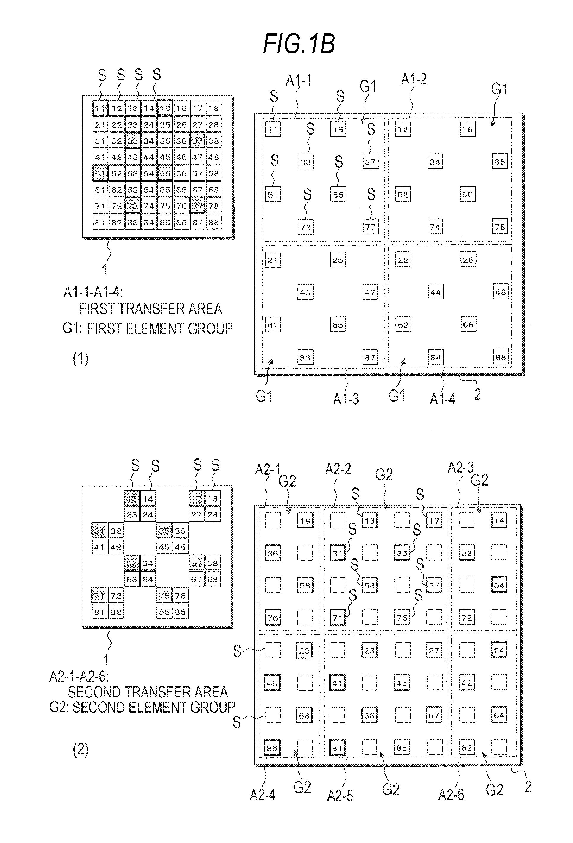
[0059]FIG. 1A to FIG. 1C are step views showing feature parts of a manufacturing method of a display device according to a first embodiment of the invention. Here, based on these drawings, a description will be made on a method of mounting light-emitting elements from a first substrate onto a second substrate in manufacture of a display device in which light-emitting elements such as light emitting diodes (LEDs) are arranged in matrix form.

[0060]Here, the first substrate is, for example, a growth substrate on which the light-emitting elements are formed or a holding substrate onto which the light-emitting elements formed and arranged on the growth substrate are temporarily mounted. The second substrate is a device substrate (wiring substrate) on which wiring or the like is provided, or a hold substrate onto which the light-emitting elements are temporarily mounted.

[0061]A description will be made on a procedure in which light-emitting elements arranged on the first substrate at init...

second embodiment

[0093]FIG. 2A to FIG. 2C are step views showing feature parts of a manufacturing method of a display device according to a second embodiment of the invention. The second embodiment is an applied example of the first embodiment. Hereinafter, similarly to the first embodiment, a method of mounting light-emitting elements from a first substrate onto a second substrate in manufacture of the display device will be described with reference to these drawings.

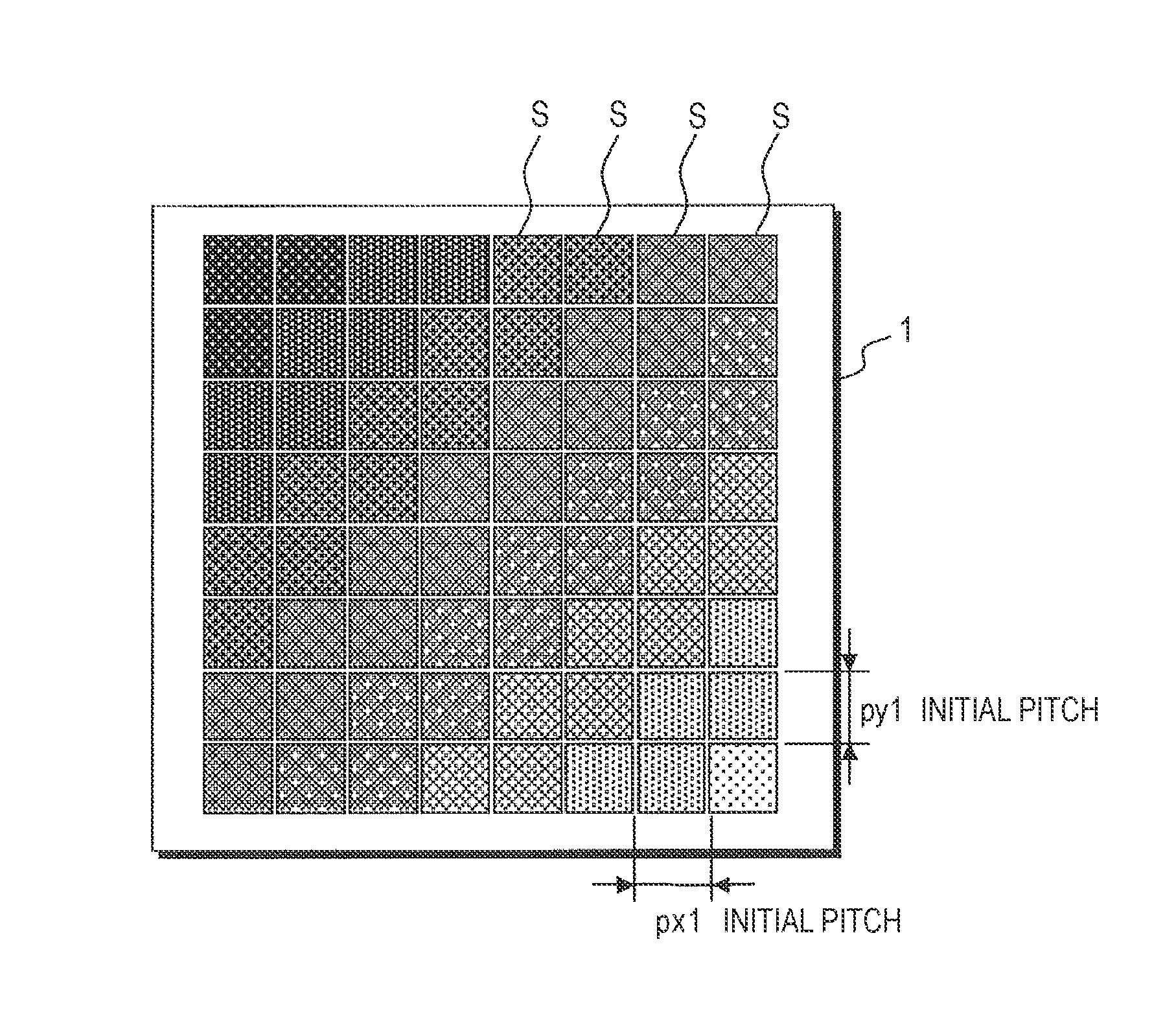
[0094]First, as shown in FIG. 2A, an in-plane distribution of emission characteristics (here, emission wavelength), such as chromaticity of emitted light or brightness, is detected with respect to plural light-emitting elements S arranged on the first substrate 1 at specified initial pitches px1 and py1.

[0095]By this, as indicated by the shading representing the emission characteristics of the respective light-emitting elements S, it is detected that the light-emitting elements S are arranged on the first substrate 1 in the distributio...

third embodiment

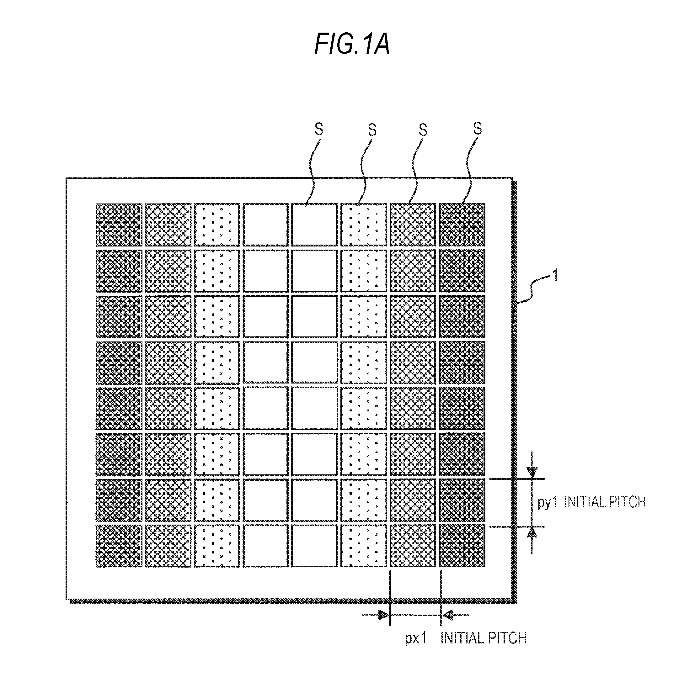
[0116]FIG. 3A to FIG. 3C are step views showing feature parts of a manufacturing method of a display device according to a third embodiment of the invention. Similarly to the first embodiment, a method of mounting light-emitting elements from a first substrate onto a second substrate in manufacture of the display device will be described with reference to these drawings.

[0117]First, as shown in FIG. 3A, an in-plane distribution of emission characteristics (here, emission wavelength), such as chromaticity of emitted light or brightness, is detected with respect to plural light-emitting elements S arranged on a first substrate 1 at specified initial pitches px1 and py1.

[0118]By this, as indicated by the shading representing the emission characteristics of the respective light-emitting elements S, it is detected that the light-emitting elements S are arranged on the first substrate 1 in the distribution where the emission characteristics are radially monotonously changed in one directi...


PUM


Abstract

A manufacturing method of a display device, includes: a first step of collectively transferring light-emitting elements arranged at every specified number of light-emitting elements formed and arranged on a first substrate to a transfer area set on a second substrate; and a second step of transferring light-emitting elements remaining on the first substrate to between the plural light-emitting elements mounted on the second substrate in at least one of a state where the first substrate is moved with respect to the transfer area on the second substrate and a state where the first substrate is rotated in a plane.

Description

BACKGROUND OF THE INVENTION[0001]1. Field of the Invention[0002]The present invention relates to a manufacturing method of a display device and a display device, and particularly to a manufacturing method of a display device in which light-emitting elements formed and arranged on a wafer are rearranged on a mounting substrate and a display device.[0003]2. Description of the Related Art[0004]In manufacture of a display device in which light emitting diodes (LEDs) are arranged in matrix form, a step is performed in which micro-size (several to several tens square) single crystal LEDs formed and arranged on a growth substrate (size of 50 to 150 mmφ) are mounted onto a device substrate. At this time, LEDs arranged at a pixel pitch period (integer times larger than an LED formation period) of the objective display device are selected from the growth substrate and are collectively transferred to the device substrate, and that is repeated, so that the display device having an objective siz...

Claims


Application Information

Patent Timeline
Patent Type & Authority Applications(United States)
IPC IPC(8): H01J1/62H01J9/20
CPCH01L25/0753H01L33/0079H01L2224/32225H01L2224/97H01L2224/83855H01L2224/83192H01L33/62H01L2924/12041H01L2224/83005H01L21/561H01L21/568H01L24/29H01L24/32H01L21/6835H01L24/83H01L24/97H01L2221/68354H01L2224/2919H01L2224/83H01L2924/00H01L33/0093
Inventor OOHATA, TOYOHARUTOMODA, KATSUHIROHIRAO, NAOKIDOI, MASATO
Owner SONY CORP
Why Eureka
Try Eureka