Method and apparatus for determining peak phase error between clock signals

a clock signal and peak phase error technology, applied in pulse manipulation, pulse technique, instruments, etc., can solve problems such as circuit failure, improper operation, and failure to opera

Active Publication Date: 2010-10-21
VIA TECH INC
View PDF31 Cites 5 Cited by
  • Summary
  • Abstract
  • Description
  • Claims
  • Application Information

AI Technical Summary

Benefits of technology

[0007]An integrated circuit according to one embodiment includes multiple clock circuits providing multiple clock signals and a peak phase error circuit. The peak phase error circuit includes phase difference logic, delay and register logic, and control logic. The phase difference logic receives a selected pair of clock signals and provides a pulse difference signal including a difference pulse indicative of a timing difference between the selected pair of clock signals. The delay and register logic has an input receiving the pulse difference signal and an output providing a peak phase error value representing peak phase error between the selected pair of clock signals. The control logic selects the pair of clock signals from among the multiple clock signals.

Problems solved by technology

Marginal or even improper PLL circuit design may, however, jeopardize successful clock domain crossing causing failure of operation.
Also, although a properly designed PLL circuit may function properly for most conditions, circuit variations and environmental conditions, such as voltage, temperature, speed, input jitter, etc., may result in improper operation and / or circuit failure.

Method used


Image

  • Method and apparatus for determining peak phase error between clock signals
  • Method and apparatus for determining peak phase error between clock signals
  • Method and apparatus for determining peak phase error between clock signals

Examples


Embodiment Construction

[0016]The following description is presented to enable one of ordinary skill in the art to make and use the present invention as provided within the context of a particular application and its requirements. Various modifications to the preferred embodiment will, however, be apparent to one skilled in the art, and the general principles defined herein may be applied to other embodiments. Therefore, the present invention is not intended to be limited to the particular embodiments shown and described herein, but is to be accorded the widest scope consistent with the principles and novel features herein disclosed.

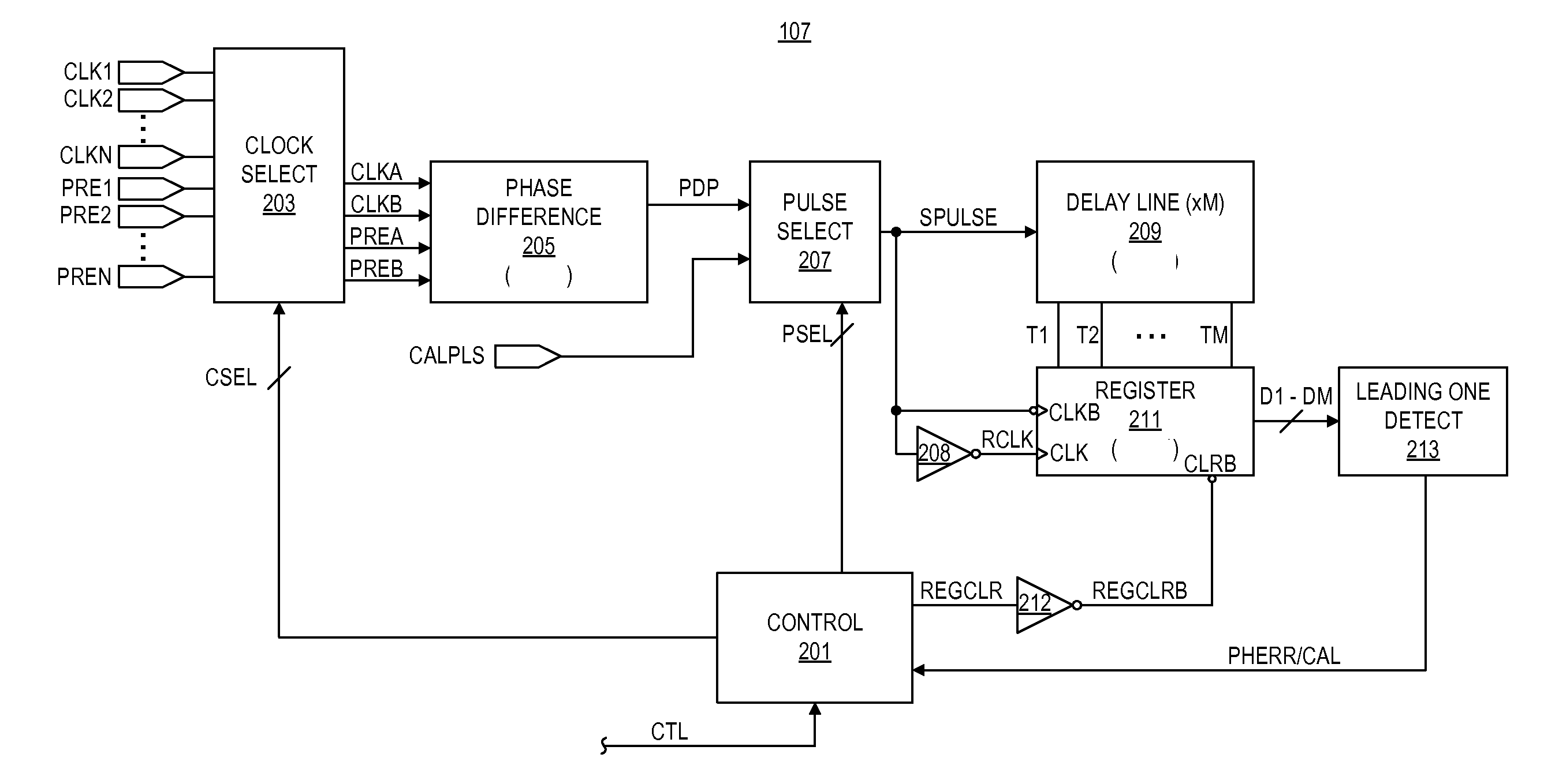
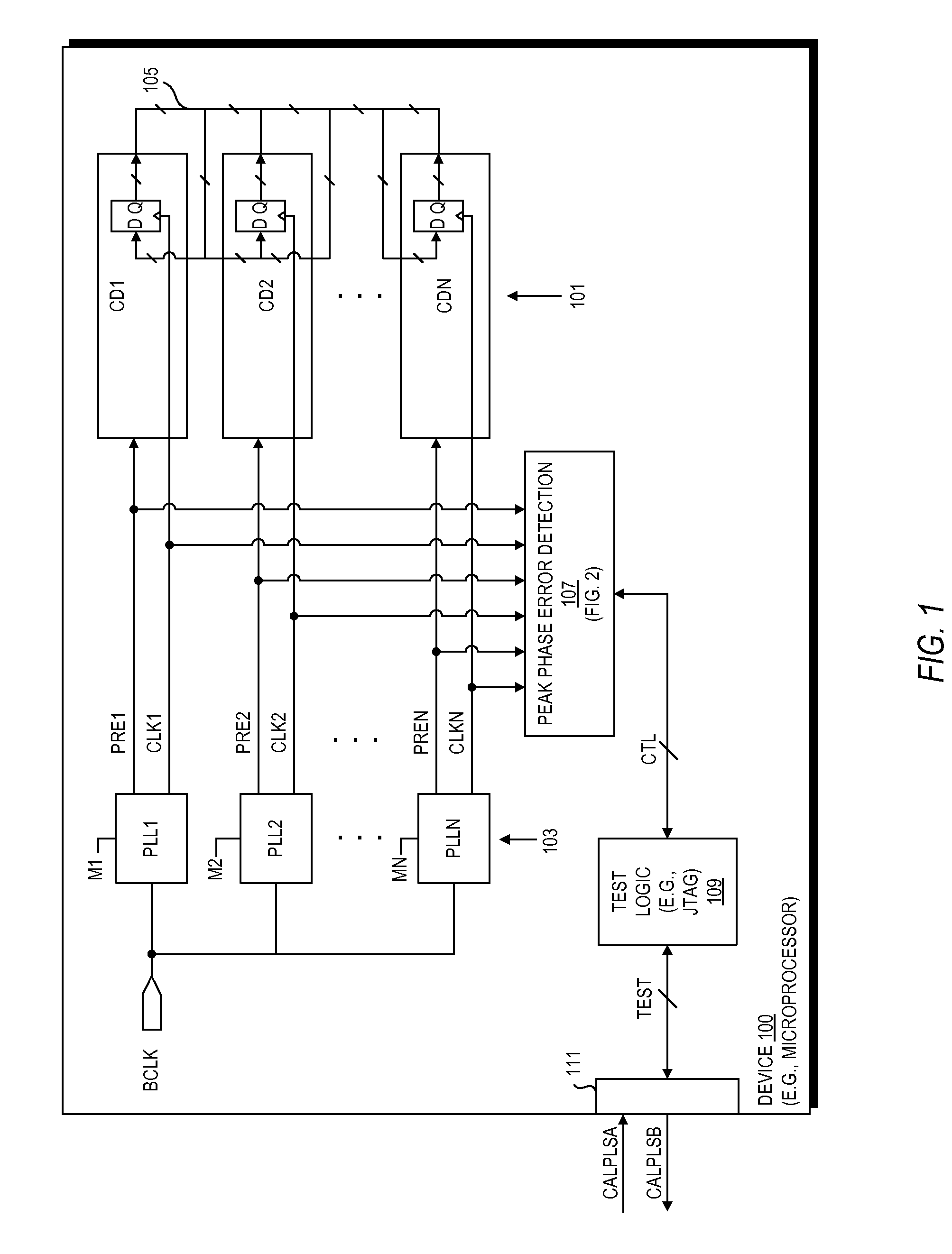
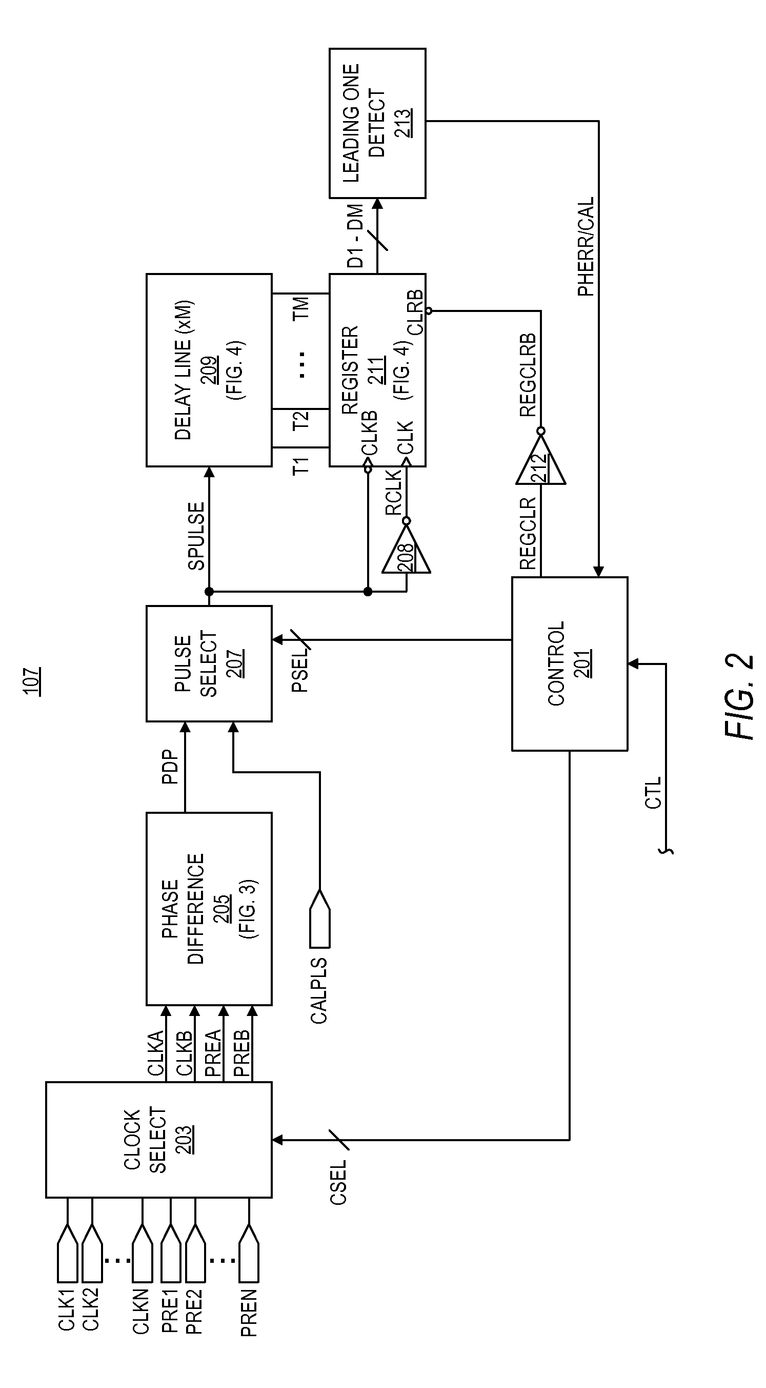
[0017]The present inventor has observed that significant variation between disparate clock signals results in improper operation. The disadvantages include, for example, improper data transfer across clock boundaries between different clock domains. She has therefore developed a method and apparatus for quantifying peak phase error between clock domains, as will be further desc...


PUM


Abstract

A peak phase error circuit including phase difference logic and delay and register logic. The phase difference logic provides a pulse difference signal including at least one difference pulse indicative of a timing difference between selected edges of a pair of clock signals. The delay and register logic receives the pulse difference signal and provides a peak phase error value representing peak phase error between the clock signals. The delay and register logic may include a delay line with multiple delay cells and taps coupled in series in which each tap provides an output state of a delay cell. The register logic registers a state of each tap to provide delay bits in response to each trailing edge of the difference pulses. Each delay bit remains set until reset so that the longest pulse difference signal is registered to provide the peak phase error.

Description

BACKGROUND OF THE INVENTION[0001]1. Field of the Invention[0002]The present invention relates to clock synchronization and clock domain crossing, and more particularly to determining peak phase error between clock signals provided to different clock domains.[0003]2. Description of the Related Art[0004]Integrated circuit design continues to advance as increased functionality is packed into shrinking circuit configurations. Different clock frequencies are used to maximize circuit efficiency for disparate circuit functions. A typical microprocessor, for example, has different clock frequencies for different circuits within different clock domains, such as a processor clock, and input / output (I / O) clock, a core clock, a bus clock, a quad-pumped clock, etc. Information must be successfully transferred between different clock domains for proper chip operation. Clock domain crossing occurs when data or information generated by a circuit within a first clock domain driven by a first clock h...

Claims


Application Information

Patent Timeline
Patent Type & Authority Applications(United States)
IPC IPC(8): G01R25/00
CPCH03L7/07H03L7/085H03L7/0814
Inventor CANAC, VANESSA S.
Owner VIA TECH INC
Why Eureka
Try Eureka