A/D converter, solid-state imaging device and camera system

a converter and solid-state imaging technology, applied in the field of a/d converters, solid-state imaging devices and camera systems, can solve the problems of difficult speeding up reading and difficult to improve operation speed, and achieve the effect of high bit precision without increasing clock frequency or reading tim

Active Publication Date: 2010-10-21
SONY CORP
View PDF5 Cites 30 Cited by
  • Summary
  • Abstract
  • Description
  • Claims
  • Application Information

AI Technical Summary

Benefits of technology

[0032]Therefore, the reading time can be reduced when the gradient of the ramp wave is made steep.
[0035]When the variation amount in each step of the ramp waves outputted by the DAC 6, namely, the step width is increased, the gradient of the ramp wave becomes steep, therefore, the reading time can be reduced without improving the operation speed of the DAC 6.
[0036]However, 1 LSB after the digital conversion is also increased merely by increasing the step width, which reduces the A / D conversion accuracy.
[0037]Thus, it is desirable to provide an A / D converter, a solid-state imaging device and a camera system capable of reducing reading time as well as realizing A / D conversion with high bit precision.
[0043]According to the embodiments of the invention, it is possible to realize A / D conversion with high bit precision without increasing a clock frequency or increasing the reading time.

Problems solved by technology

However, it is not easy to improve the operation speed of the DAC 6 which is an analog circuit while maintaining the precision, therefore, it is difficult to speedup the reading.

Method used


Image

  • A/D converter, solid-state imaging device and camera system
  • A/D converter, solid-state imaging device and camera system
  • A/D converter, solid-state imaging device and camera system

Examples


Embodiment Construction

[0057]Hereinafter, embodiments of the invention will be explained with reference to the drawings.

[0058]The explanation will be made in the following order.

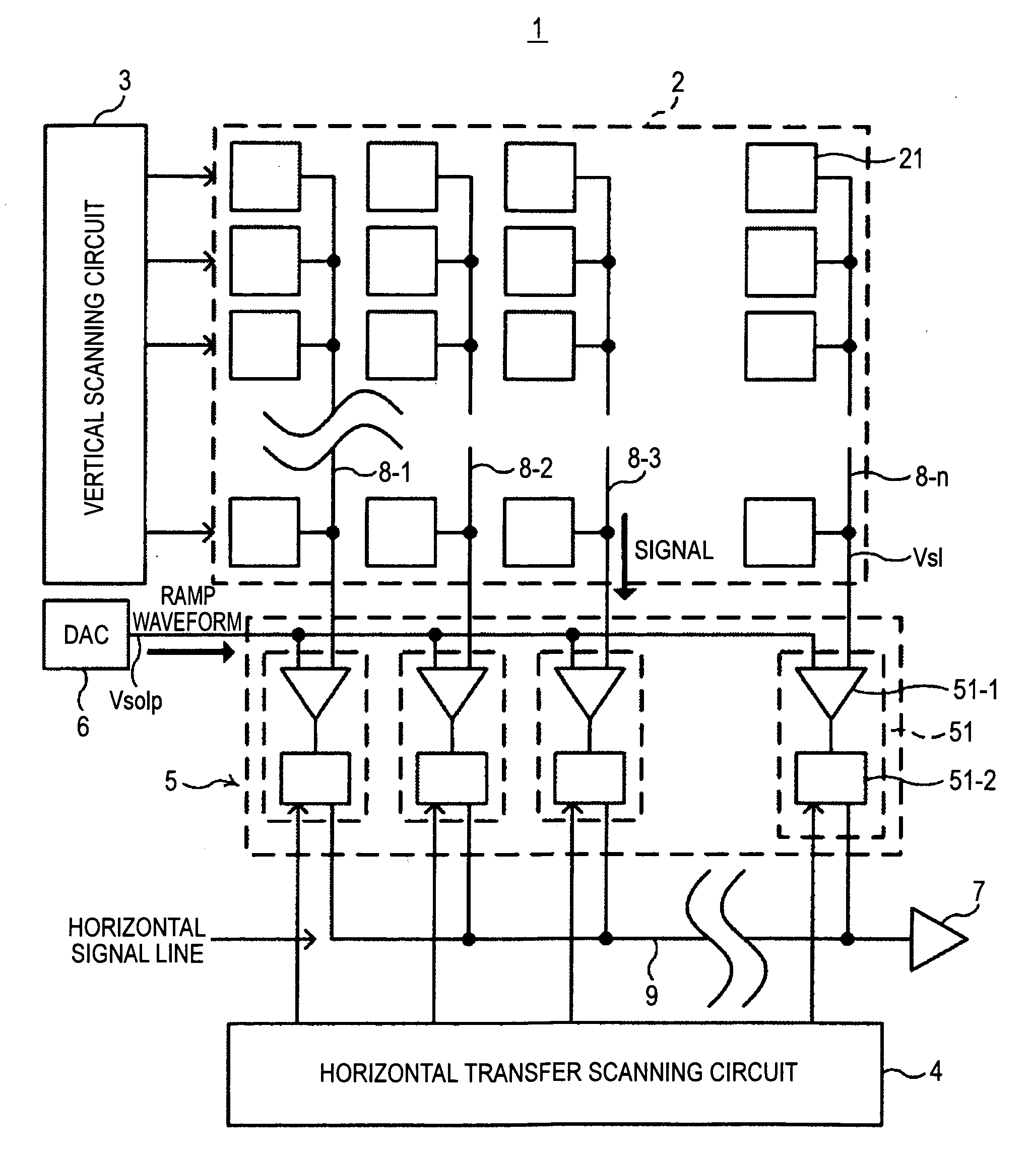
1. Entire configuration example of a solid-state imaging device

2. Configuration example of a column ADC

3. Example of forming plural reference voltages by a DAC

4. Configuration example of a camera system

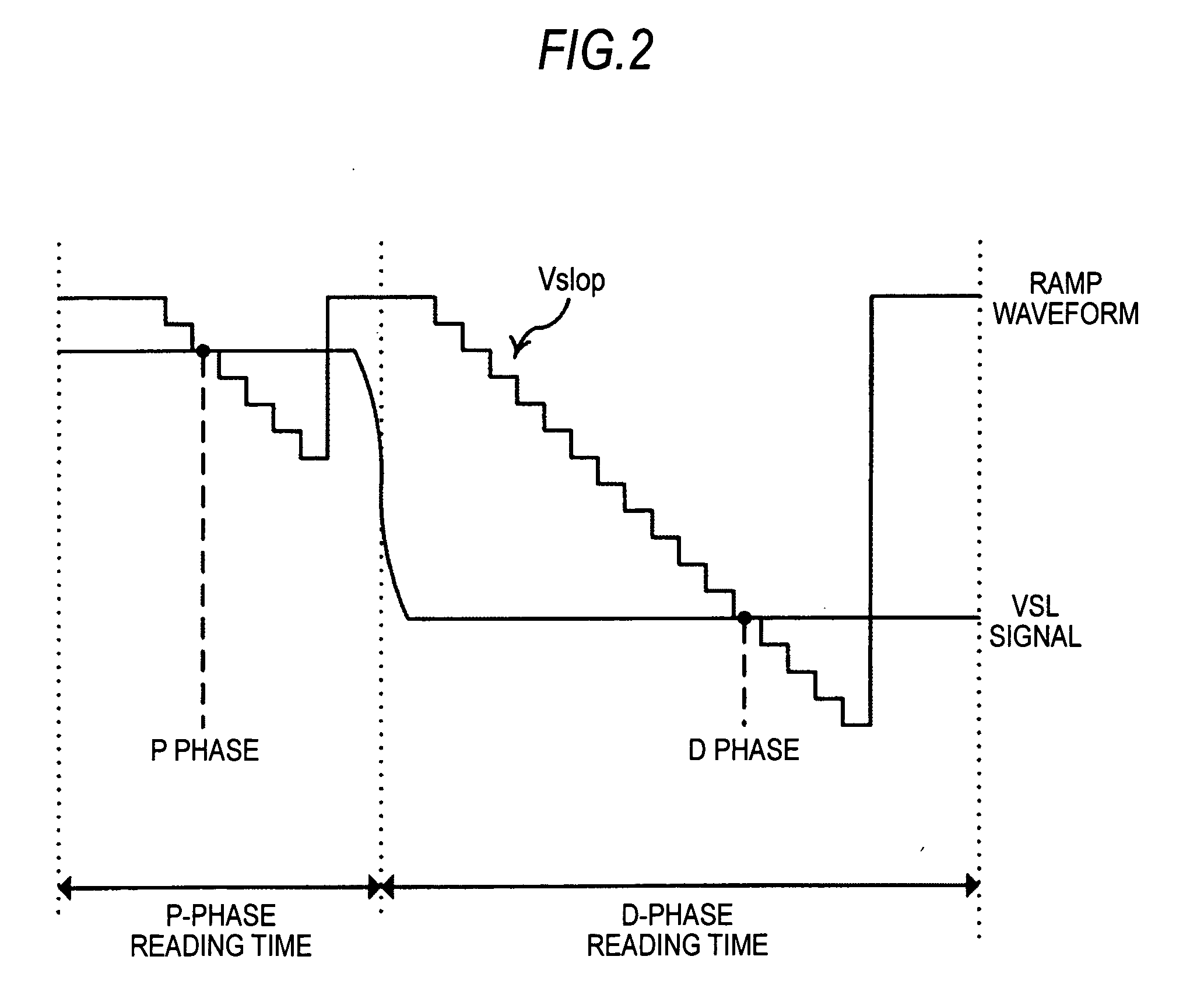
[0059]FIG. 3 is a block diagram showing a configuration example of a column-parallel ADC mounted solid-state imaging device (CMOS image sensor) according to an embodiment of the invention.

[0060]FIG. 4 is a block diagram more specifically showing an ADC group in the column-parallel ADC mounted solid-state imaging device (CMOS image sensor) of FIG. 3.

1. Entire Configuration Example of a Solid-State Imaging Device

[0061]A solid-state imaging device 100 includes a pixel section 110 as an imaging section, a vertical scanning circuit 120, a horizontal transfer scanning circuit 130 and a timing control circuit 140 as shown in FIG. 3 and FIG...


PUM


Abstract

An A / D converter includes: plural comparators to which reference voltages as ramp waves different from each other are supplied, which are configured to compare the supplied reference voltages with an analog input signal; and plural latches arranged so as to correspond to the plural comparators, which are configured to count comparison time of the corresponding comparators, to stop counting when an outputs of the comparator is inverted and to store the count value, wherein the plural reference voltages are offset by an arbitrary voltage at the same time point.

Description

BACKGROUND OF THE INVENTION[0001]1. Field of the Invention[0002]The present invention relates to an A / D converter which can be applied to a solid-state imaging device typified by a CMOS image sensor, a solid-state imaging device and a camera system.[0003]2. Description of the Related Art[0004]As for the CMOS image sensor, the same manufacturing process as common CMOS-type integrated circuits can be used for the manufacture thereof as well as driving can be performed by a single power source, and further, an analog circuit and a logic circuit using the CMOS process can be mixed on the same chip.[0005]Accordingly, the CMOS image sensor has plural big advantages such that the number of peripheral ICs can be reduced.[0006]The mainstream of a CCD output circuit is 1-ch output using a FD amplifier having a floating diffusion layer (FD).[0007]On the other hand, the CMOS image sensor has FD amplifiers at respective pixels, the mainstream of the output is a column-parallel output type in whi...

Claims


Application Information

Patent Timeline
Patent Type & Authority Applications(United States)
IPC IPC(8): H04N5/335H03M1/12H04N5/369H04N5/374H04N5/378
CPCH03M1/0678H03M1/1023H03M1/123H03M1/34H04N5/378H01L27/146H03M1/12H03M1/56H04N25/75
Inventor NISHI, TAKAFUMI
Owner SONY CORP
Why Eureka
Try Eureka