[0009]It is therefore an object of the present invention to provide an optical device wafer
processing method which can prevent the damage to an optical device wafer in
spite of its reduced thickness and can divide the wafer into individual optical devices without the deposition of minute broken pieces onto the surface of each optical device.
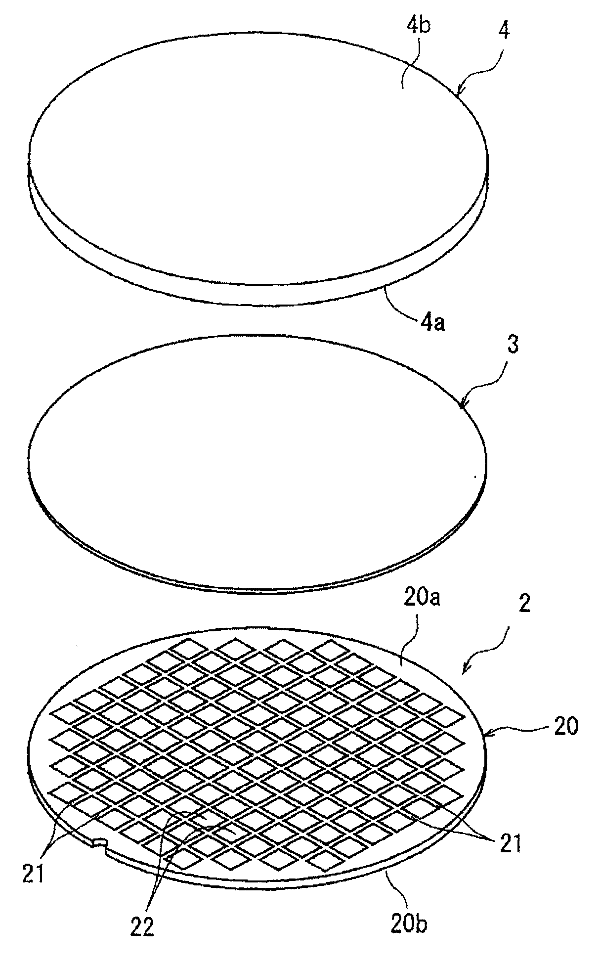
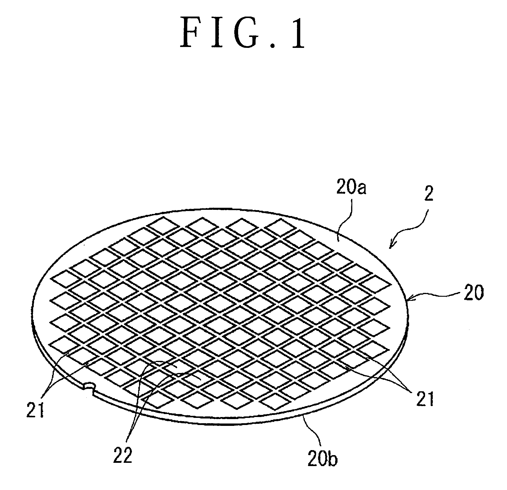
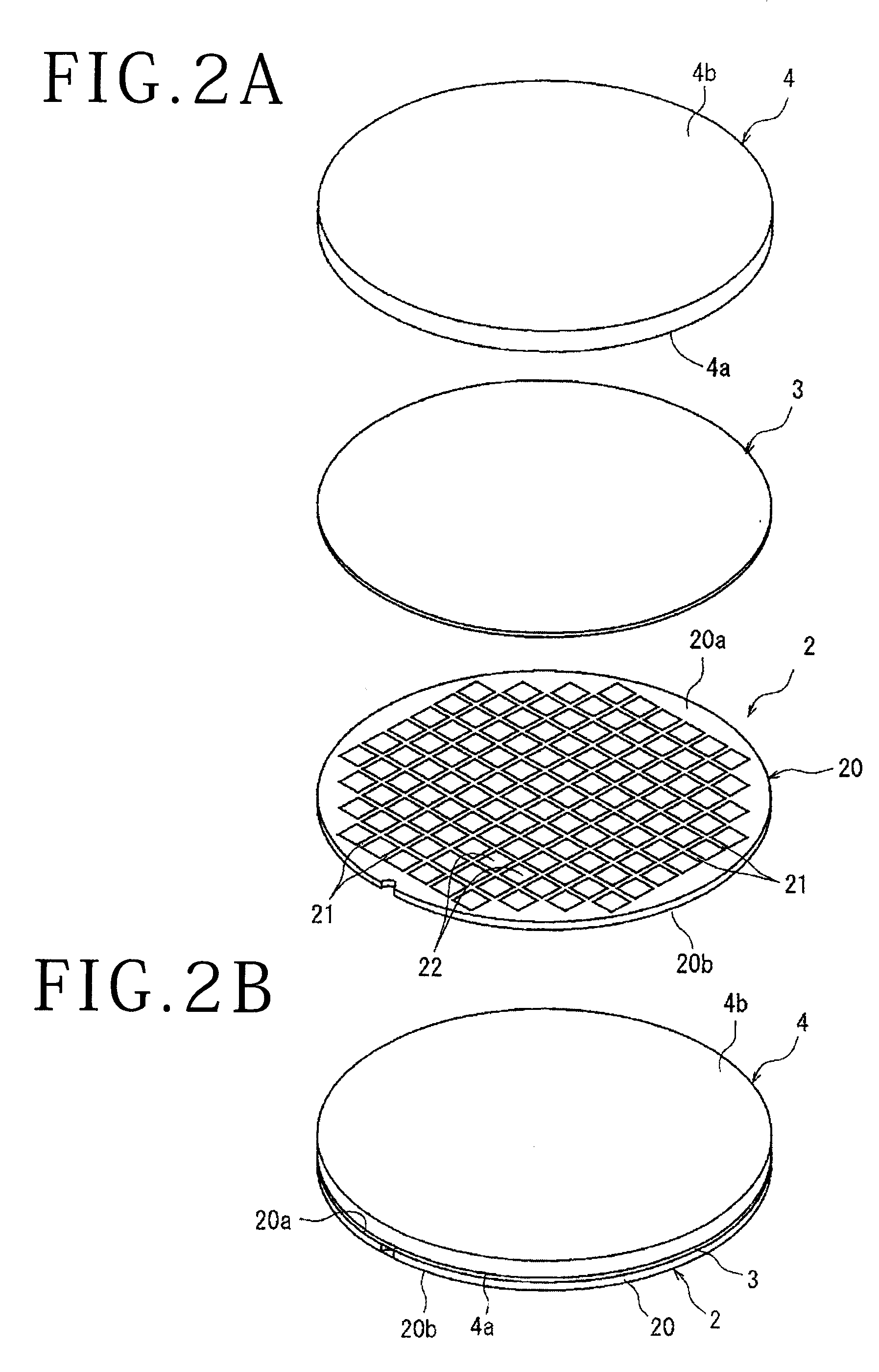
[0010]In accordance with an aspect of the present invention, there is provided an optical device wafer processing method for dividing an optical device wafer into individual optical devices along a plurality of crossing streets formed on the front side of a sapphire substrate constituting the optical device wafer, the individual optical devices being respectively formed in a plurality of regions partitioned by the streets, the optical device wafer processing method including: a protective plate attaching step of removably attaching a rigid protective plate through a double-sided adhesive tape to the front side of the sapphire substrate, the protective plate being formed from a transparent member, the double-sided adhesive tape being composed of a sheet capable of blocking
ultraviolet radiation and first and second adhesive
layers formed on both sides of the sheet, wherein the adhesive force of each adhesive layer of the double-sided adhesive tape can be reduced by applying
ultraviolet radiation; a sapphire substrate
grinding step of grinding the back side of the sapphire substrate to reduce the thickness of the sapphire substrate to a predetermined finished thickness of each optical device after performing the protective plate attaching step; a modified layer forming step of applying a
laser beam having a transmission
wavelength to the sapphire substrate along the streets from the back side of the sapphire substrate with a focal
point set inside the sapphire substrate to thereby form a modified layer inside the sapphire substrate along each street after performing the sapphire substrate grinding step; a wafer supporting step of attaching the back side of the sapphire substrate to a
dicing tape supported to an annular frame after performing the modified layer forming step; a protective plate removing step of applying
ultraviolet radiation through the protective plate to the double-sided adhesive tape to thereby reduce the adhesive force of the first adhesive layer of the double-sided adhesive tape formed on the protective plate side and removing the protective plate from the double-sided adhesive tape in the condition where the double-sided adhesive tape is left on the front side of the sapphire substrate after performing the wafer supporting step; and a wafer dividing step of applying an external force to the sapphire substrate to thereby break the sapphire substrate along each street where the modified layer is formed, thus dividing the wafer into the individual optical devices after performing the protective plate removing step.
[0011]Preferably, the optical device wafer processing method further includes a double-sided adhesive tape removing step of applying
ultraviolet radiation through the
dicing tape and the sapphire substrate to the double-sided adhesive tape to thereby reduce the adhesive force of the second adhesive layer of the double-sided adhesive tape formed on the sapphire substrate side and removing the double-sided adhesive tape from the sapphire substrate after performing the wafer dividing step; and a
pickup step of picking up the individual optical devices divided from each other and attached to the dicing tape from the dicing tape after performing the double-sided adhesive tape removing step.
[0012]In the optical device wafer processing method according to the present invention, the sapphire substrate grinding step of grinding the back side of the sapphire substrate constituting the optical device wafer to reduce the thickness of the sapphire substrate to a predetermined finished thickness of each optical device is performed after performing the protective plate attaching step of attaching the rigid protective plate through the double-sided adhesive tape to the front side of the sapphire substrate. Accordingly, although the thickness of the sapphire substrate is reduced to 50 μm or less, for example, there is no possibility of
cracking in the sapphire substrate because the rigid protective plate is attached to the front side of the sapphire substrate.
[0013]Further, also in performing the modified layer forming step and the wafer supporting step after the sapphire substrate grinding step, there is no possibility of damage to the very thin sapphire substrate because the rigid protective plate is attached to the front side of the sapphire substrate.
[0014]In the wafer dividing step, an external force is applied to the sapphire substrate attached to the dicing tape in the condition where the double-sided adhesive tape is left on the front side of the sapphire substrate after performing the protective plate removing step, thereby breaking the sapphire substrate along each street where the modified layer is formed. Thus, the wafer is divided into the individual optical devices in the condition where the double-sided adhesive tape is attached to the front side of the sapphire substrate. When the sapphire substrate of the wafer is broken along each street so as to start from the modified layer serving as a break starting portion, minute broken pieces may scatter. However, the minute broken pieces adhere to the double-sided adhesive tape attached to the front side of the sapphire substrate, so that they are prevented from being deposited onto each optical device.

