Decontamination of mocvd chamber using nh3 purge after in-situ cleaning

a technology of in-situ cleaning and mocvd chamber, which is applied in the direction of coatings, chemical vapor deposition coatings, solid-state devices, etc., can solve the problems of affecting process reproducibility and uniformity, process cumbersomeness, and process conditions that dri

Inactive Publication Date: 2010-10-28
APPLIED MATERIALS INC
View PDF62 Cites 132 Cited by
  • Summary
  • Abstract
  • Description
  • Claims
  • Application Information

AI Technical Summary

Benefits of technology

[0010]Embodiments of the present invention generally relate to methods and apparatus for removing unwanted deposition build-up from one more interior surfaces of a substrate processing chamber after a substrate is processed in a chamber to form, for example, Group III-V materials by metal-organic chemical vapor deposition (MOCVD) deposition processes and / or hydride vapor phase epitaxial (HVPE) deposition processes. In one embodiment, a method for removing unwanted deposition build-up from one or more interior surfaces of a metal organic chemical vapor deposition (MOCVD) processing chamber is provided. The method comprises depositing one or more Group III containing layers over a substrate disposed in the processing chamber, transferring the substrate out of the processing chamber, pulsing a halogen cleaning gas into the processing chamber to remove at least a portion of the unwanted deposition build-up from one or more interior surfaces of the processing chamber, and pulsing a purge gas into the processing chamber after pulsing the halogen cleaning gas to remove reaction by-products formed from the reaction of the halogen cleaning gas with the unwanted deposition build-up from the processing chamber, wherein the pulsing a purge gas immediately follows the pulsing a halogen cleaning gas to remove reaction by-products from the interior surfaces of the processing chamber before the reaction by-products condense on the interior surface of the substrate processing chamber.
[0011]In another embodiment, a method for removing unwanted deposition build-up from one or more interior surfaces of a substrate processing chamber is provided. The method comprises positioning a substrate on a susceptor in a processing region of a substrate processing chamber comprising a showerhead for supplying processing gases to the processing region, depositing one or more gallium containing layers over the substrate disposed in the processing region, transferring the substrate out of the substrate processing chamber, pulsing chlorine gas into the substrate processing chamber to remove at least a portion of the unwanted deposition build-up from one or more interior surfaces and the showerhead of the substrate processing chamber, and pulsing a first purge gas into the processing chamber to remove the chlorine gas and reaction by-products formed from the reaction of the chlorine gas with the unwanted deposition build-up from the substrate processing chamber.
[0012]In yet another embodiment, an integrated processing system for manufacturing compound nitride semiconductor devices is provided. The integrated processing system comprises one or more substrate processing chambers operable to form one or more Group III compound nitride semiconductor layers on one or more substrates positioned in the substrate processing chamber, a halogen gas source coupled with at least one of the one or more substrate processing chambers operable for pulsing a halogen gas into the substrate processing chamber to remove at least a portion of unwanted deposition build-up deposited when forming one or more Group III compound nitride semiconductor layers on the one or more substrates from one or more interior surfaces of the substrate processing chambers, and a purge gas source coupled with at least one of the one or more substrate processing chamber operable for pulsing purge gas into the one or more substrate processing chamber to remove reaction by-products formed from the reaction of the halogen gas with the unwanted deposition build-up from the substrate processing chamber.

Problems solved by technology

Such unwanted deposition may create particles and flakes within the chamber, resulting in the drift of process conditions and more importantly affecting the process reproducibility and uniformity.
This is a very cumbersome process, and represents an unreasonable limitation on any high-throughput, substrate processing system.

Method used


Image

  • Decontamination of mocvd chamber using nh3 purge after in-situ cleaning
  • Decontamination of mocvd chamber using nh3 purge after in-situ cleaning
  • Decontamination of mocvd chamber using nh3 purge after in-situ cleaning

Examples


Embodiment Construction

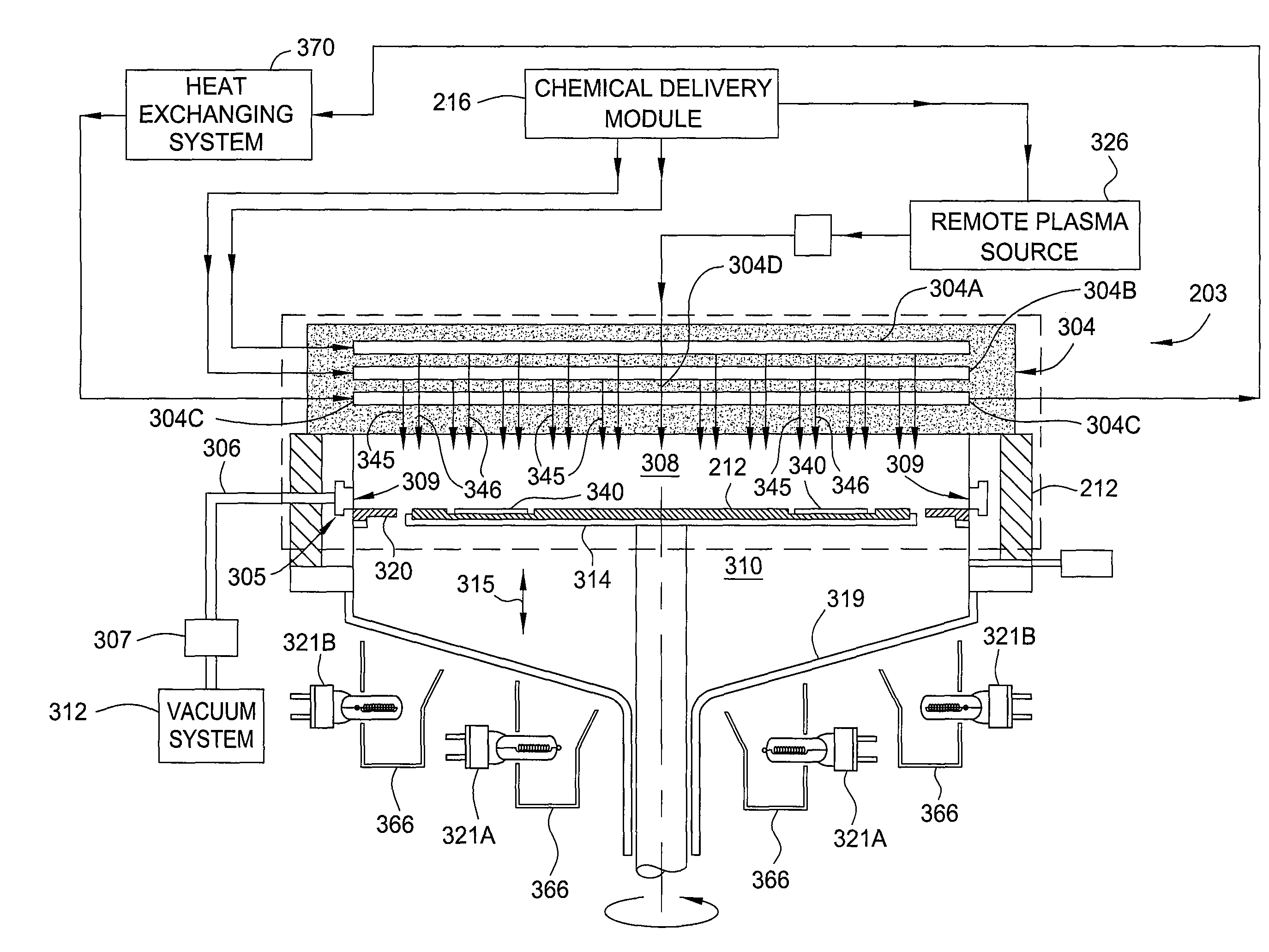
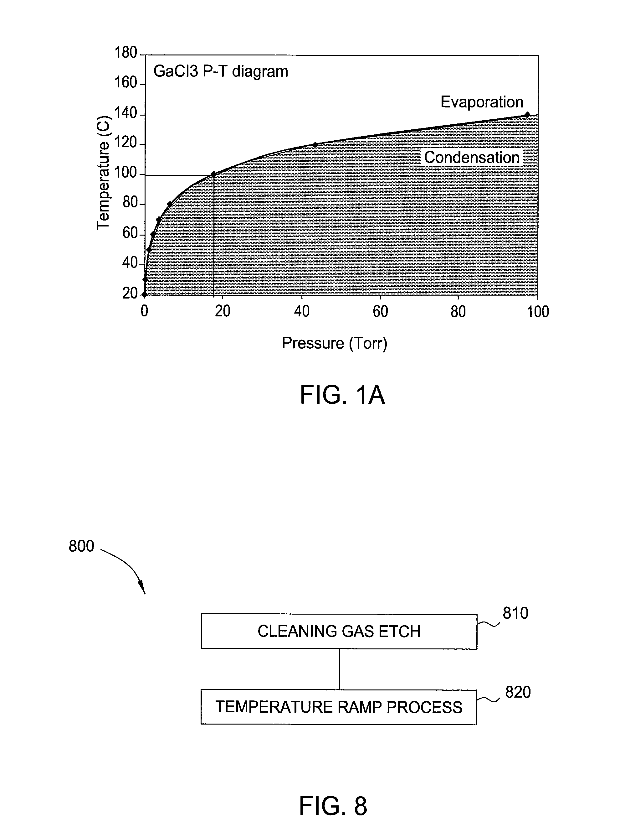
[0028]Embodiments described herein provide improved methods and apparatus for chamber cleaning which may be performed in-situ to remove unwanted deposition build-up off the interior surfaces of a substrate processing chamber thus reducing particle contamination while maintaining system uptime. In one embodiment, the chamber cleaning process is performed by pulsing a halogen containing gas, such as chlorine containing cleaning gas, into the substrate processing chamber to convert the unwanted deposition, such as gallium coating, on the surfaces of the chamber and the chamber components into a gaseous form, such as GaCl3, which may then be removed from the chamber.

[0029]As previously discussed, the growth of high temperature GaN by MOCVD or HVPE often results in severe parasitic deposition on chamber parts especially the showerhead. This parasitic deposition causes particles and flaking inside the chamber, resulting in drift of the process conditions, and most importantly affecting th...


PUM

PropertyMeasurementUnit
timeaaaaaaaaaa
timeaaaaaaaaaa
timeaaaaaaaaaa

Abstract

Embodiments of the present invention generally relate to methods and apparatus for removing unwanted deposition build-up from one more interior surfaces of a substrate processing chamber after a substrate is processed in a chamber to form, for example, Group III-V materials by metal-organic chemical vapor deposition (MOCVD) deposition processes and/or hydride vapor phase epitaxial (HVPE) deposition processes. In one embodiment, a method for removing unwanted deposition build-up from one or more interior surfaces of a substrate processing chamber is provided. The method comprises depositing one or more Group III containing layers over a substrate disposed in the substrate processing chamber, transferring the substrate out of the substrate processing chamber, and pulsing a halogen containing gas into the substrate processing chamber to remove at least a portion of the unwanted deposition build-up from one or more interior surfaces of the substrate processing chamber.

Description

CROSS-REFERENCE TO RELATED APPLICATIONS[0001]This application claims benefit of U.S. provisional patent application Ser. No. 61 / 173,552 (14309L), filed Apr. 28, 2009, which is herein incorporated by reference it its entirety.BACKGROUND OF THE INVENTION[0002]1. Field of the Invention[0003]Embodiments of the present invention generally relate to methods and apparatus for removing unwanted deposition build-up from one or more interior surfaces of a substrate processing chamber after a substrate is processed in the chamber to form, for example, Group III-V materials by metal-organic chemical vapor deposition (MOCVD) deposition processes and / or hydride vapor phase epitaxial (HVPE) deposition processes.[0004]2. Description of the Related Art[0005]Group III-V films are finding greater importance in the development and fabrication of a variety of semiconductor devices, such as short wavelength Light-emitting diodes (LEDs), laser diodes (LDs), and electronic devices including high power, hig...

Claims


Application Information

Patent Timeline
Patent Type & Authority Applications(United States)
IPC IPC(8): H01L51/40
CPCC23C16/303C23C16/4405C23C16/45563H01L33/007H01L21/0237H01L21/0254H01L21/0262C23C16/45574H01L33/02
Inventor KRYLIOUK, OLGASU, JIEGRIFFIN, KEVINJUN, SUNG WONNIJWAHAN, SANDEEPDONG, XIZIPOON, TZEWASHINGTON, LORI D.GRAYSON, JACOB
Owner APPLIED MATERIALS INC
Why Eureka
Try Eureka