

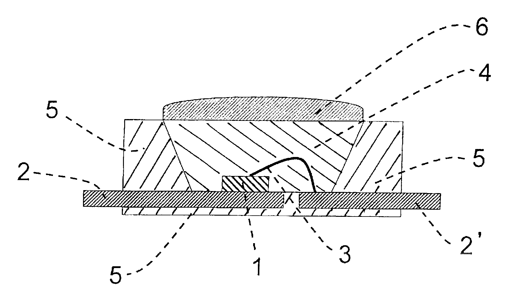
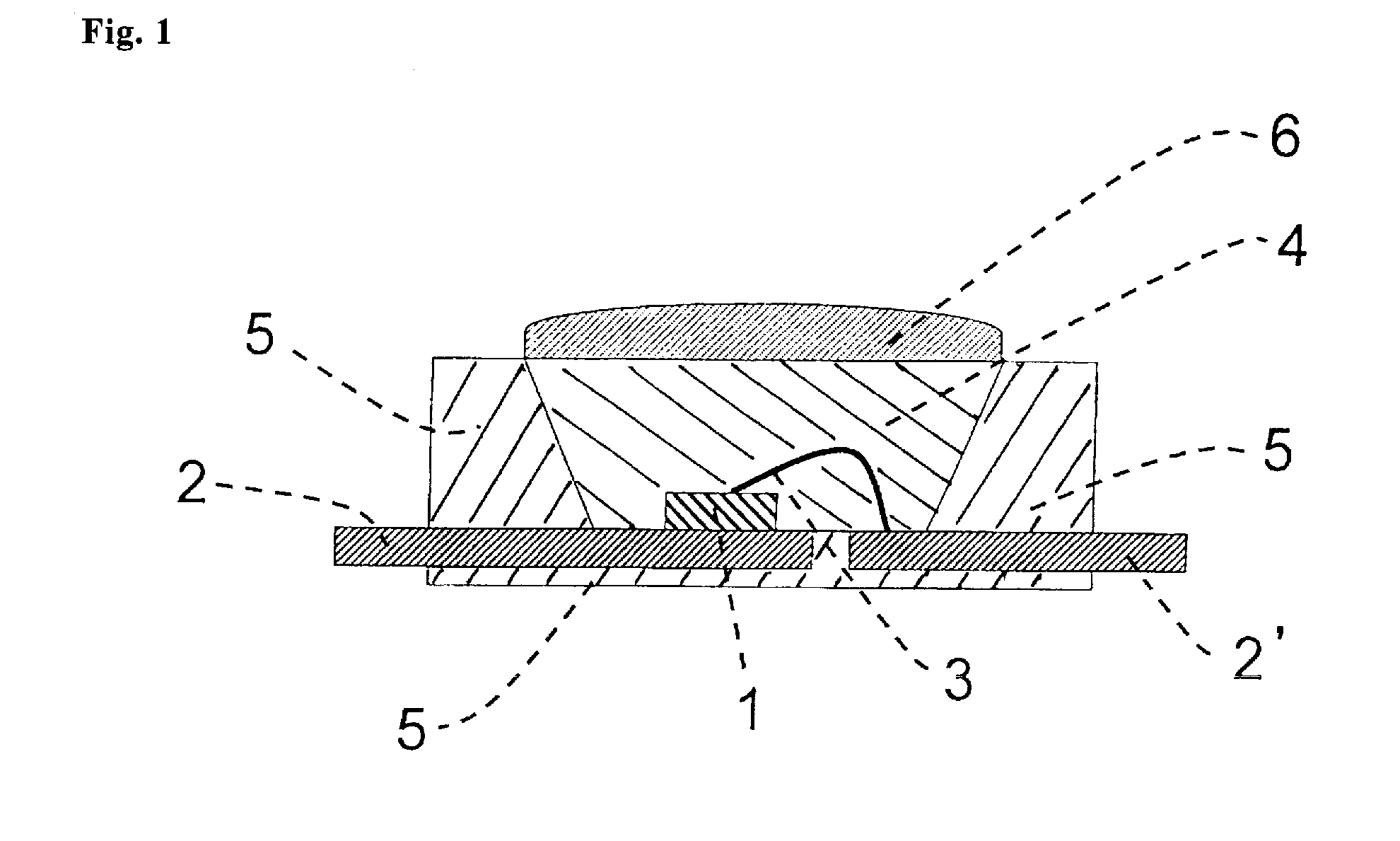
Silicone resin composition for optical semiconductor devices and an optical semiconductor device
a technology of optical semiconductors and silicon resins, applied in the direction of semiconductor/solid-state device details, solid balls, sport apparatus, etc., can solve the problems of insufficient light resistance of the composition, yellowing problem, low light output, etc., and achieve excellent adhesion and anti-cracking, poor crack resistance, and high stiffness
- Summary
- Abstract
- Description
- Claims
- Application Information
AI Technical Summary
Benefits of technology
Problems solved by technology
Method used
Image

Examples
synthesis example 1
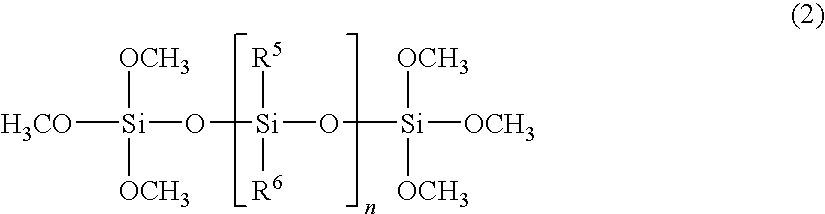
Organopolysiloxane (A)
[0071]To a one-litter flask were added 100 grams of methyltrichlorosilane and 200 grams of toluene. To the resulting mixture, was added dropwise a mixture of 8 grams of water and 60 grams of isopropyl alcohol over 5 to 20 hours while keeping the inner temperature at −5 to 0 degrees C. by cooling the flask in an ice bath. Then, the mixture was heated at a refluxing temperature for 20 minutes with stirring, and cooled to room temperature, to which 12 grams of water were added dropwise at a temperature below 30 degrees C. over 30 minutes and the mixture was stirred for 20 minutes. Further, 25 grams of water were added dropwise and stirred at a temperature of 40 to 45 degrees C. for 60 minutes. Then, 200 grams of water were added and an organic phase was separated. The organic phase was washed until the phase became neutral and then subjected to azeotropic dehydration, filtration, and strip under reduced pressure to obtain 36.0 grams of a colorless and transparent ...
synthesis example 2
Organopolysiloxane (F)
[0077]5.4 Grams (0.03 mole) of phenylmethyldichlorosilane, 114 grams (0.539 mole) of phenyltrichlorosilane, 100 grams (0.066 mole) of a silicone oil having 20 Si atoms and chlorodimethyl groups on both ends and represented by Cl(Me)2SiO(Me2SiO)nSi (Me)2Cl wherein n is 18 on average, 3000 grams of toluene were mixed, added dropwise to 11000 grams of water, and hydrolyzed at a temperature of 30 to 50 degrees C. for 1 hour. Then, the mixture was aged at 50 degrees C. for 1 hour, to which water was added for washing. Then, the organic phase was subjected to azeotropic dehydration, filtration, and strip under reduced pressure to obtain colorless and transparent organopolysiloxane (F) which had a melt viscosity of 5 Pa·s at 150 degrees C. and is represented by the following formula (9). The content of the silanol group was 3 mole %.
(G) Linear Diorganopolysiloxane
[0078]
[0079]n=900 to 1000, ex Shin-Etsu Chemical Co., Ltd.
Additives
PUM
| Property | Measurement | Unit |
|---|---|---|
| particle diameter | aaaaa | aaaaa |
| moldability | aaaaa | aaaaa |
| wavelengths | aaaaa | aaaaa |
Abstract
Description
Claims
Application Information