Multilayer structure comprising a phase change material layer and method of producing the same

a phase change material and multi-layer structure technology, applied in the direction of bulk negative resistance effect devices, basic electric elements, electrical instruments, etc., can solve the problems of local temperature increase, flash memory scaling beyond 45 nm nodes, and the inability to realize the known process of producing phase change memories

Active Publication Date: 2010-11-04
NXP BV
View PDF7 Cites 3 Cited by
  • Summary
  • Abstract
  • Description
  • Claims
  • Application Information

AI Technical Summary

Benefits of technology

[0009]It may be an object of the invention to provide a multilayer structure comprising a phase change material layer and a method of prod...

Problems solved by technology

In the field of non-volatile memories, flash memory scaling beyond a 45 nm node has become a real issue.
A high current density caused by the pulse may lead to a local temperature increase.
However,...

Method used


Image

  • Multilayer structure comprising a phase change material layer and method of producing the same
  • Multilayer structure comprising a phase change material layer and method of producing the same
  • Multilayer structure comprising a phase change material layer and method of producing the same

Examples


Embodiment Construction

[0032]The illustration in the drawing is schematically. In different drawings, similar or identical elements are provided with similar or identical reference signs.

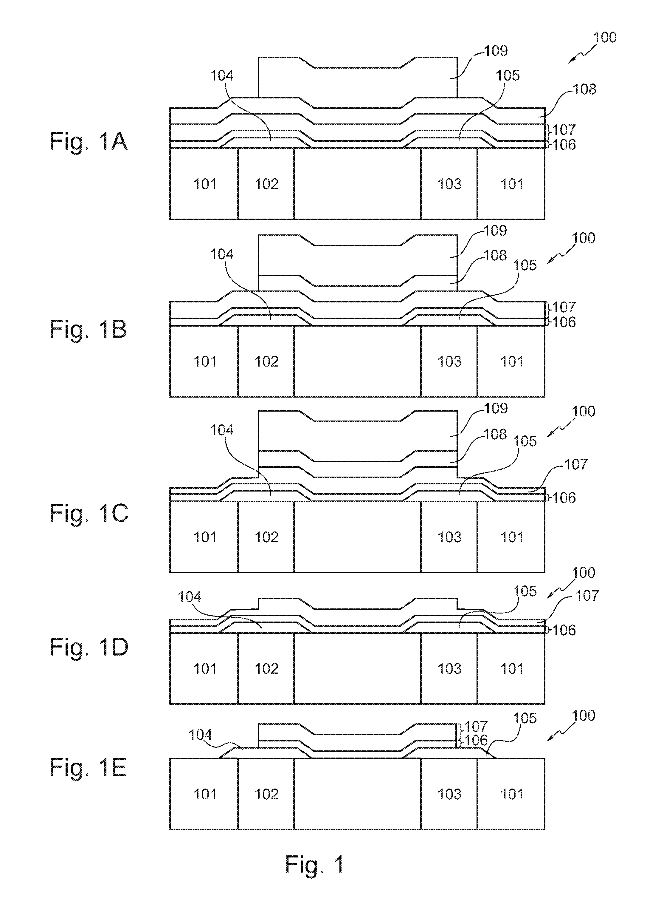
[0033]FIG. 1 shows a schematically process flow for patterning a phase change material layer according to a first exemplary embodiment of the invention. In particular, Fig. 1A shows a multilayer structure 100 which may be a part of a memory cell, wherein the multilayer structure 100 comprises a base layer 101 and two conductor paths 102 and 103 burrowed in the substrate 101 or formed by a damascene process. The conductor paths may be formed of metal, e.g. copper. The conductor paths 102 and 103 are connected to electrodes 104 and 105, respectively, which may be formed by tantalum-nitride (TaN) for example. On the substrate 101 and the electrodes 104 and 105 a phase change material (PCM) layer 106 is formed e.g. by using GeTe-Sb2Te3 such as Ge2Sb2Te5. Onto the PCM layer 106 a protective layer 107, e.g. a protective insulat...


PUM


Abstract

A method of producing a multilayer structure is provided, wherein the method comprises forming a phase change material layer onto a substrate, forming a protective layer, forming a further layer on the protective layer, patterning the further layer in an first 5 patterning step, patterning the protective layer and the phase change material layer by a second patterning step. In particular, the first patterning step may be an etching step using chemical etchants. Moreover, electrodes may be formed on the substrate before the phase change material layer is formed, e.g. the electrodes may be formed on one level, e.g. may forma planar structure and may not form a vertically structure.

Description

FIELD OF THE INVENTION[0001]The invention relates to a multilayer structure comprising a phase change material layer, in particular to a memory cell comprising a phase change material layer.[0002]The invention further relates to a method of producing a multilayer structure comprising a phase change material layer.BACKGROUND OF THE INVENTION[0003]In the field of non-volatile memories, flash memory scaling beyond a 45 nm node has become a real issue. Technologies to face this challenge are ferroelectric, magnetic and phase change memories, the latter one being promising for the replacement of flash and showing characteristics that may allow replacement of other types of memories such as DRAM. Phase change memories are a possible solution for the unified memory being an important step in the electronics art. OTP (“on time programmable”) and MTP (“multiple times programmable”) memories open a field that may present a great opportunity for phase change memories as well.[0004]Phase change...

Claims


Application Information

Patent Timeline
IPC IPC(8): H01L45/00H01L21/02
CPCH01L45/06H01L45/1675H01L45/144H01L45/1226H10N70/231H10N70/823H10N70/8828H10N70/063
Inventor DELHOUGNE, ROMAINLISONI, JUDITPARASCHIV, VASILE
Owner NXP BV
Why Eureka
Try Eureka