Method for fabricating flexible semiconductor device and layered film used therefore

Active Publication Date: 2010-11-04
PANASONIC CORP
View PDF4 Cites 9 Cited by
  • Summary
  • Abstract
  • Description
  • Claims
  • Application Information

AI Technical Summary

Benefits of technology

[0023]According to the present invention, the layered film including the first metal layer, the inorganic insulating layer, the semiconductor layer, and the second metal layer which are sequentially formed is used as a base structure, the first metal layer and the second metal layer are processed to for

Problems solved by technology

Moreover, formation of such TFT elements using a Si material involves a high-temperature process, adding a limitation on a substrate material that the substrate material needs to be resistant to the process temperature.
Note that a quartz substrate may be used, but the quartz substrate is expensive, which is economi

Method used


Image

  • Method for fabricating flexible semiconductor device and layered film used therefore
  • Method for fabricating flexible semiconductor device and layered film used therefore
  • Method for fabricating flexible semiconductor device and layered film used therefore

Examples


embodiment 1

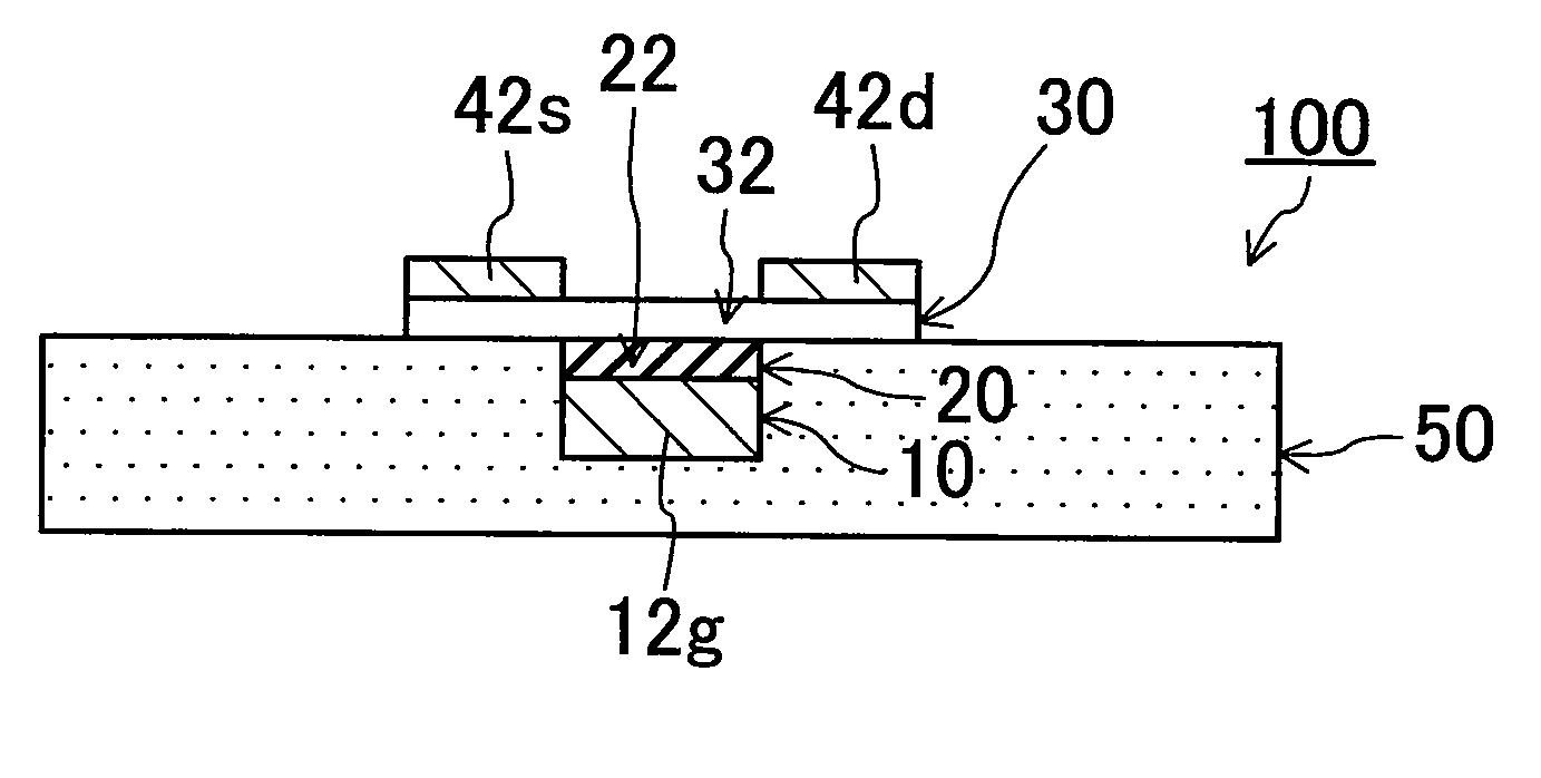
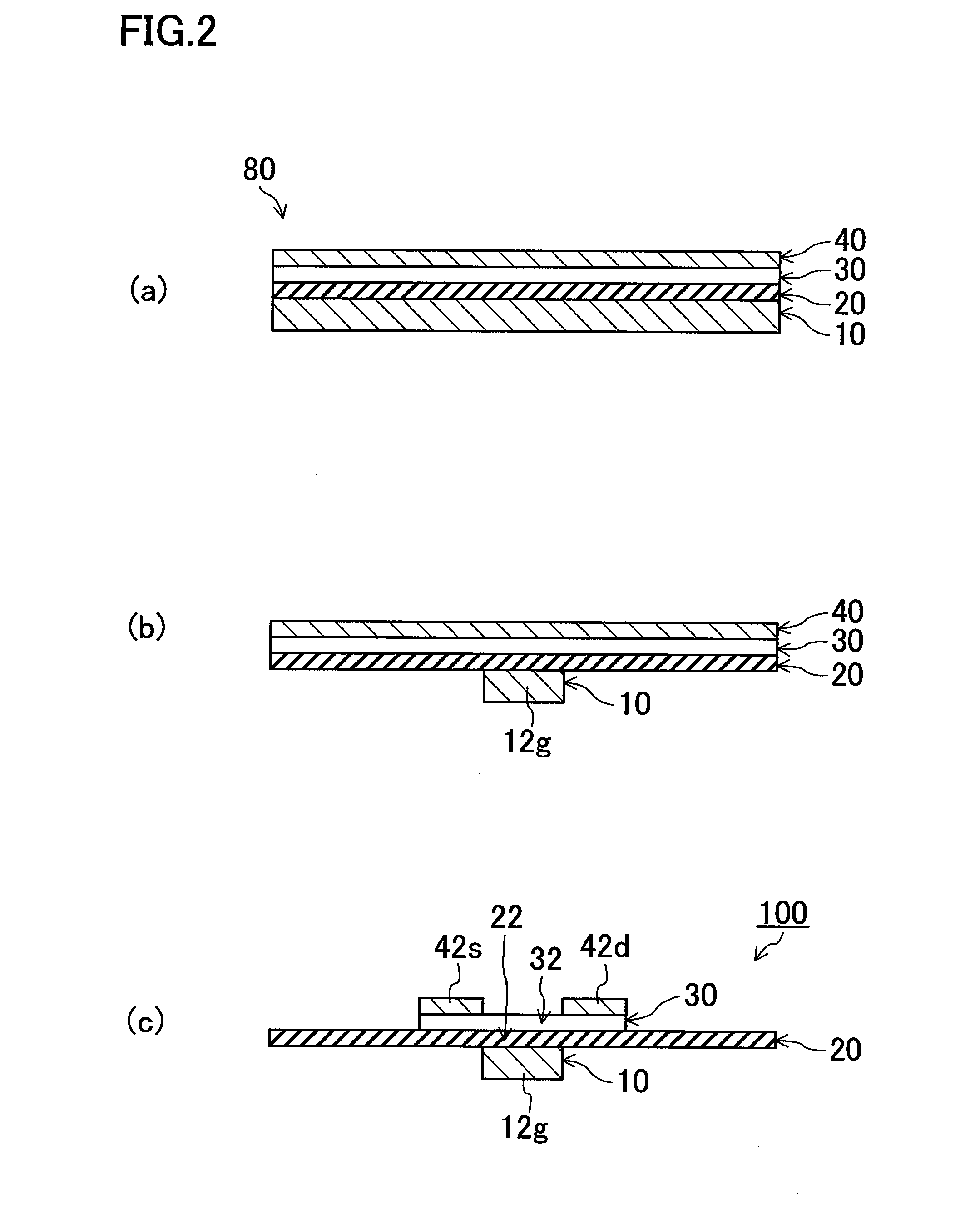
[0052]FIGS. 2(a)-2(c) are cross-sectional views illustrating basic processes in a method for fabricating a flexible semiconductor device 100 according to Embodiment 1 of the present invention.

[0053]First, as illustrated in FIG. 2(a), a layered film 80 is prepared, where the layered film 80 includes a first metal layer 10, an inorganic insulating layer 20, a semiconductor layer 30, and a second metal layer 40 which are sequentially formed. Here, the first metal layer 10 and the second metal layer 40 may be made of either the same material or different materials. Although the inorganic insulating layer 20 may be made of any material, the inorganic insulating layer is desirably a thin film having a high relative dielectric constant because the inorganic insulating layer functions as a gate insulating film of a thin film transistor. Moreover, the semiconductor layer 30 may be made of any material, but the semiconductor layer 30 is desirably a thin film having a high carrier mobility bec...

embodiment 2

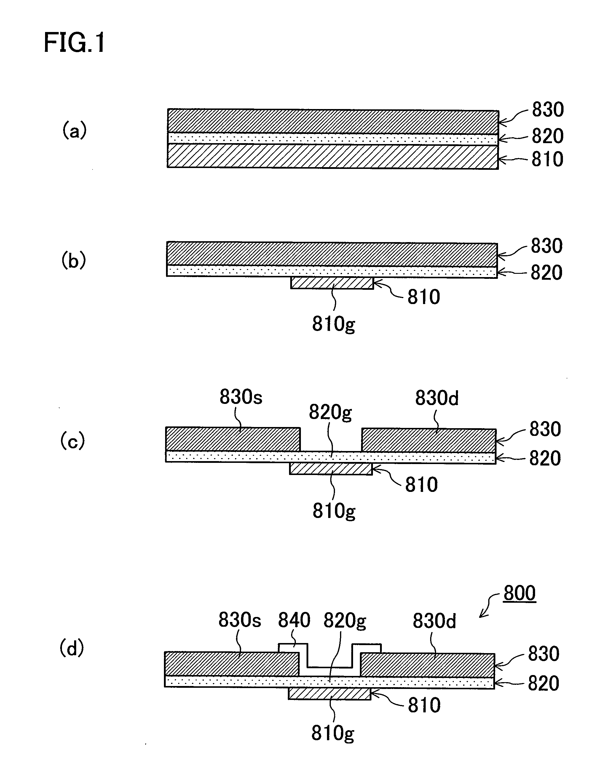
[0099]FIG. 7 illustrates a configuration of a flexible semiconductor device 200 according to Embodiment 2 of the present invention. Embodiment 2 is different form Embodiment 1 in that an interlayer connector 60a connected to a gate electrode 12g is not a paste via but a plating via. The plating via 60a is formed in a resin sheet 50 after a layered film 80 and the resin sheet 50 are integrally laminated. With reference to FIGS. 8(a)-8(d), an example fabrication process of the flexible semiconductor device 200 will be described. Note that the same description as that in Embodiment 1 other than matters particularly described in Embodiment 2 will be omitted.

[0100]First, as illustrated in FIG. 8(a), a layered film 80 is prepared, where the layered film 80 includes a first metal layer 10, an inorganic insulating layer 20, a semiconductor layer 30, and a second metal layer 40 which are sequentially formed.

[0101]Next, as illustrated in FIG. 8(b), the first metal layer 10 of the layered film...

embodiment 3

[0107]FIG. 9 illustrates a configuration of a flexible semiconductor device 300 according to Embodiment 3 of the present invention. Embodiment 3 differs from Embodiment 1 in that an anti-diffusion layer (barrier layer) 90 is provided. In Embodiment 3, the anti-diffusion layer 90 is provided between a source electrode 42s and a semiconductor layer 32 and between a drain electrode 42d and the semiconductor layer 32. The source electrode 42s and the drain electrode 42d are made of copper, and the anti-diffusion layer 90 is made of tantalum nitride (TaN). In the illustrated embodiment, the anti-diffusion layer 90 is provided not only under lower surfaces of the source electrode 42s and the drain electrode 42d but also under a lower surface of wiring 44.

[0108]Copper (Cu) has the property of easily dispersing in a semiconductor material (e.g., silicon) at a high temperature of several hundred degrees Celsius or above. Therefore, in the case where the source electrode 42s and the drain ele...


PUM


Abstract

A method for fabricating a flexible semiconductor device includes: preparing a layered film 80 including a first metal layer 10, an inorganic insulating layer 20, a semiconductor layer 30, and a second metal layer 40 which are sequentially formed; etching the first metal layer 10 to form a gate electrode 12g; compression bonding a resin layer 50 to a surface of the layered film 80 provided with the gate electrode 12g to allow the gate electrode 12g to be embedded in the resin layer 50; and etching the second metal layer 40 to form a source electrode 42s and a drain electrode 42d, wherein the inorganic insulating layer 20 on the gate electrode 12g functions as a gate insulating film 22, and the semiconductor layer 30 between the source electrode 42s and drain electrode 42d on the inorganic insulating layer 20 functions as a channel 32.

Description

RELATED APPLICATIONS[0001]This application is the U.S. National Phase under 35 U.S.C. §371 of International Application No. PCT / JP2009 / 003440, filed on Jul. 22, 2009, which in turn claims the benefit of Japanese Application No. 2008-239121, filed on Sep. 18, 2008, the disclosures of which Applications are incorporated by reference herein.TECHNICAL FIELD[0002]The present invention relates to methods for fabricating flexible semiconductor devices and layered films used therefore.BACKGROUND ART[0003]With popularization of information terminals, there has been a growing demand for flat panel displays as computer displays. Moreover, with progress in information technology, information conventionally provided on a paper medium has been increasingly provided as electronic data. Electronic paper or digital paper has therefore been increasingly demanded as a thin, lightweight, easily portable mobile display medium (for example, PATENT DOCUMENT 1).[0004]Generally, in flat panel displays, disp...

Claims


Application Information

Patent Timeline
IPC IPC(8): H01L29/786H01L21/336H01L21/77
CPCH01L24/18H01L27/1218H01L29/66765H01L29/78603H01L29/78609H01L29/78681H01L29/7869H01L51/0024H01L51/003H01L51/0097H01L51/0541H01L51/0545H01L2221/68377H01L2224/18H01L2224/76155H01L2224/82039H01L2224/92144H01L2924/01002H01L2924/01004H01L2924/01013H01L2924/01015H01L2924/0102H01L2924/01029H01L2924/0103H01L2924/01032H01L2924/01033H01L2924/01038H01L2924/01049H01L2924/01056H01L2924/01057H01L2924/01073H01L2924/01078H01L2924/01082H01L2924/04941H01L2924/04953H01L2924/10329H01L2924/19041H01L2924/30105H01L2924/01005H01L2924/01006H01L2924/0104H01L2924/01047H01L2924/01072H01L2924/01019H01L2224/82102H01L24/82H01L2924/15788H01L2924/12042H01L2224/04105H01L2224/73267H01L2224/92244H01L24/19Y02E10/549Y02P70/50H10K71/50H10K71/80H10K77/111H10K10/466H10K10/464H01L2924/00H01L27/1214H01L29/4908
Inventor ICHIRYU, TAKASHINAKATANI, SEIICHIHIRANO, KOICHIYAMASHITA, YOSHIHISAKOMATSU, SHINGO
Owner PANASONIC CORP
Why Eureka
Try Eureka