Electronic package structure

a technology of electronic components and packaging, applied in the direction of final product manufacturing, electrical apparatus construction details, stress/warp reduction of printed circuits, etc., can solve the problems of electronic components, electronic products operating, and damage to materials having different thermal expansion coefficients, so as to improve the integrity of electronic packages and reduce the defect rate , the effect of prolonging the service li

Inactive Publication Date: 2010-11-04
NATIONAL TSING HUA UNIVERSITY
View PDF5 Cites 4 Cited by
  • Summary
  • Abstract
  • Description
  • Claims
  • Application Information

AI Technical Summary

Benefits of technology

[0009]Via the abovementioned technical scheme, the present invention features a higher integrity electronic package, a lower defect rate, and a longer service life.
[0010]The SMA connection portions of the present invention can absorb the deformation caused by different thermal expansion coefficients of different elements during thermal cycles and can restore the shape thereof via heating, whereby the integrity of the electronic package and the electronic elements thereinside and is maintained. Therefore, the present invention can reduce the defect rate and prolong the service life of the product.

Problems solved by technology

In addition to external mechanical damage, thermal stress also causes the damage of electronic components.
The thermal stress generated by the operation of electronic products will damage the materials having different thermal expansion coefficients.
The waste heat generated by an electronic product will cause the expansion of the chip and substrate, which is likely to induce the materials fatigue in the concentration points of thermal stress.
After a long time of use, the bonding between the UBM layers and the solder bumps may disconnect, or the tin-based solderballs may be cracked or delaminated.

Method used


Image

  • Electronic package structure
  • Electronic package structure
  • Electronic package structure

Examples


Embodiment Construction

[0022]Below, the technical contents of the present invention are described in detail with the embodiments. However, it should be understood that the embodiments are only to exemplify the present invention but not to limit the scope of the present invention.

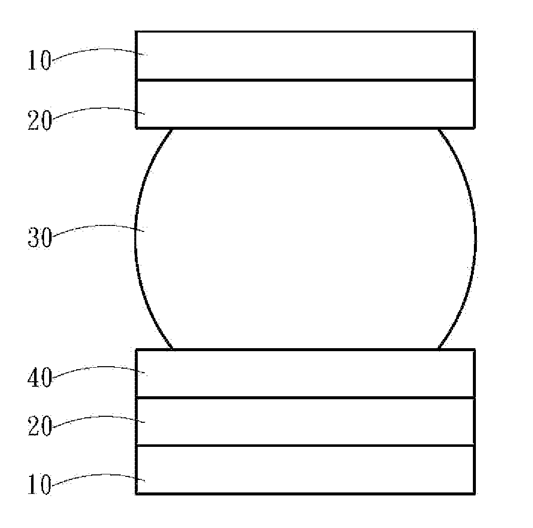
[0023]Refer to FIG. 5, a diagram schematically showing an electronic package structure according to one embodiment of the present invention. The present invention proposes an electronic package structure, which comprises an electronic element 10, a plurality of SMA (Shape Memory Alloy) connection portions 20, and a plurality of solder connection members 30. One side of the SMA connection portion 20 is bonded to the electronic element 10, and the solder connection member 30 is arranged over the other side of the SMA connection portion 20. The SMA connection portions 20 may be made of a nickel-titanium SMA, a titanium-iron SMA, nickel-iron SMA, or a titanium-copper SMA. In the embodiment of the present invention, the SMA connection ...


PUM


Abstract

The present invention discloses an electronic package structure, which comprises an electronic element, a plurality of SMA (Shape Memory Alloy) connection portions, and a plurality of solder connection members. One side of the SMA connection portion is joined to the electronic element, and the solder connection member is arranged over the other side of the SMA connection portion. The SMA connection portions can comply with the strains caused by thermal stresses during the operation of the electronic product and can restore the original shape after the thermal stresses disappear. Therefore, the preset invention can prevent the junctions between the SMA connection portions and the electronic element/the solder connection members from the crack or disconnection caused by thermal stresses.

Description

FIELD OF THE INVENTION[0001]The present invention relates to an electronic package manufacturing process, particularly to an electronic package manufacturing process using a shape memory alloy.BACKGROUND OF THE INVENTION[0002]The objective of electronic package is to connect the chip with the substrate, protect the chip, and enhance the strength and stability of the chip. In addition to external mechanical damage, thermal stress also causes the damage of electronic components. Refer to Fig.1, a diagram schematically showing the thermal stress-induced damage of a conventional electronic product. In the conventional flip chip technology, a chip 1 is bonded to a substrate 2 with a plurality of tin-based solderball 3, and a resin 4 is filled into the gap therebetween, whereby the size of an electronic product can be greatly reduced.[0003]The thermal stress generated by the operation of electronic products will damage the materials having different thermal expansion coefficients. For exa...

Claims


Application Information

Patent Timeline
Patent Type & Authority Applications(United States)
IPC IPC(8): H01R12/00
CPCH01R4/01H05K1/0271H05K3/244H05K2201/2045H05K3/4015H05K2201/068H05K3/3436Y02P70/50
Inventor DUH, JENQ-GONGTAN, CHIA-YEN
Owner NATIONAL TSING HUA UNIVERSITY
Why Eureka
Try Eureka