Soi substrate and method for manufacturing soi substrate

a technology which is applied in the field of soi substrate, can solve the problems of transfer defects, insufficient bonding strength of silicon substrate and quartz substrate, and easy deformation of yield, so as to improve the surface condition of the soi layer, prevent transfer defects, and increase yield

Inactive Publication Date: 2010-11-18
SHIN ETSU CHEM IND CO LTD
View PDF4 Cites 95 Cited by
  • Summary
  • Abstract
  • Description
  • Claims
  • Application Information

AI Technical Summary

Benefits of technology

[0030]In the present invention, the thickness of the silicon dioxide film provided on the single-crystal silicon substrate and the correlation between the thickness of the silicon dioxide film and the depth of formation of the ion-implanted layer have been optimized. Consequently, it is possible to prevent any transfer defects or slip dislocation from occurring in a

Problems solved by technology

According to a study made by the present inventor et al., however, it has become evident that the yield easily degrades noticeably in a step of silicon thin film separation performed in succession to the bonding together of a silicon substrate and a quartz substrate if an attempt is made to fabricate an SOQ substrate using the above-described SmartCut method or a method

Method used


Image

  • Soi substrate and method for manufacturing soi substrate
  • Soi substrate and method for manufacturing soi substrate
  • Soi substrate and method for manufacturing soi substrate

Examples


embodiments

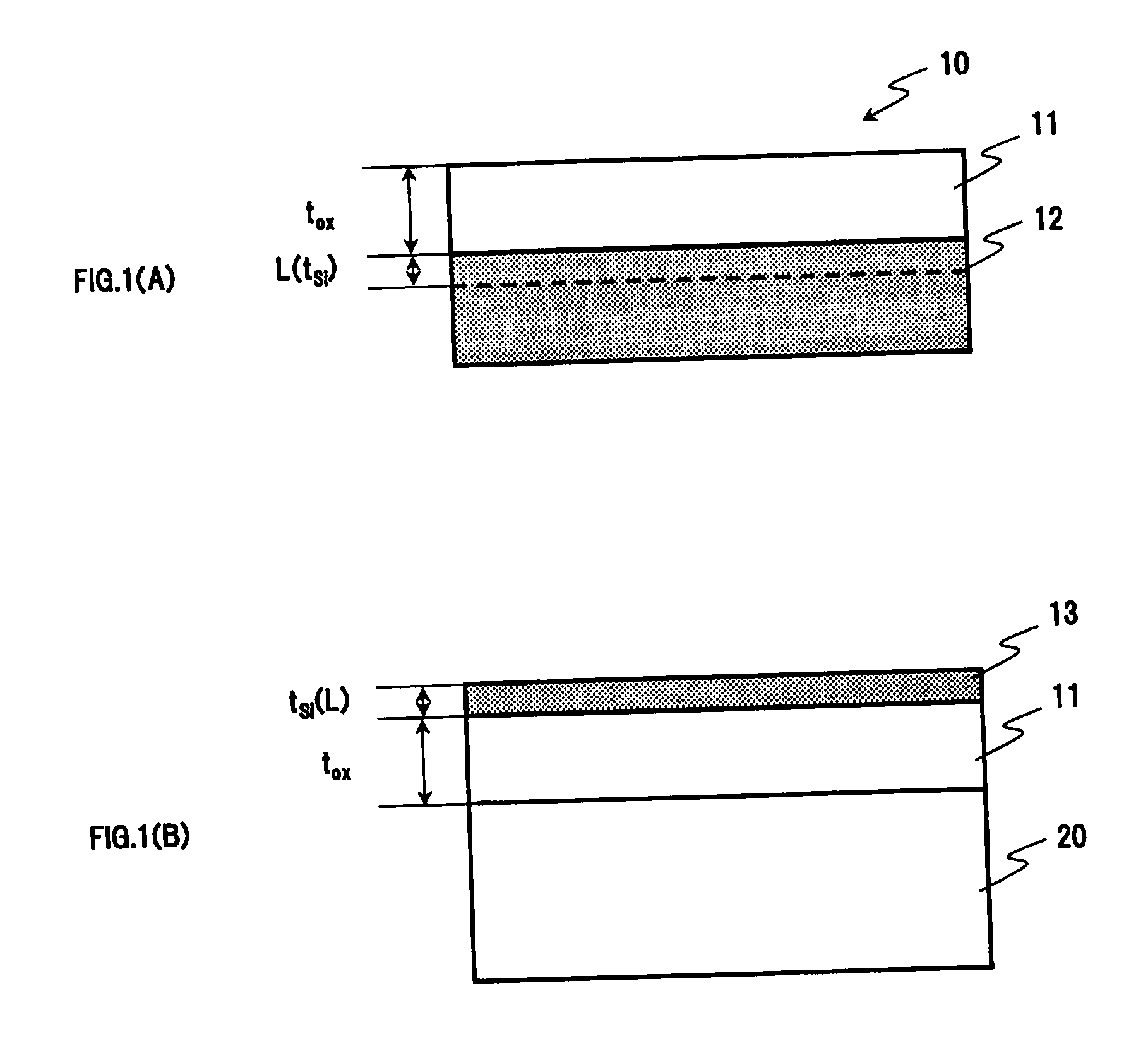
[0052]FIG. 4 is a schematic view used to explain a process example of a method for manufacturing an SOI substrate according to the present invention, wherein a first substrate 10 illustrated in FIG. 4(A) is a single-crystal Si substrate and a second substrate 20 is a quartz substrate. Here, the single-crystal Si substrate 10 is, for example, a commercially-available Si substrate grown by the Czochralski (CZ) method. The electrical property values, such as the conductivity type and specific resistivity, the crystal orientation and the crystal diameter of the single-crystal Si substrate 10 are selected as appropriate depending on the design value and process of a device to which the SOI substrate manufactured using the method of the present invention is devoted or on the display area of a device to be manufactured. Note that, as described above, an oxide film 11 is previously formed by means of, for example, thermal oxidation on a surface (bonding surface) of this single-crystal Si su...


PUM


Abstract

An oxide film having a thickness “tox” of not less than 0.2 μm is provided on the bonding surface of a single-crystal silicon substrate. In a method for manufacturing an SOI substrate according to the present invention, a low-temperature process is employed to suppress the occurrence of thermal strain attributable to a difference in the coefficient of thermal expansion between the silicon substrate and a quartz substrate. To this end, the thickness “tox” of the oxide film is set to a large value of not less than 0.2 μm to provide sufficient mechanical strength to the thin film to be separated and, at the same time, to allow strain to be absorbed in and relaxed by the relatively thick oxide film to suppress the occurrence of transfer defects during the step of separation.

Description

TECHNICAL FIELD[0001]The present invention relates to an SOI substrate having a single-crystal silicon thin film on a quartz substrate which is a transparent insulating substrate and to a method for manufacturing the SOI substrate.BACKGROUND ART[0002]An SOQ (silicon-on-quartz) substrate having a silicon thin film on a quartz substrate is an SOI substrate which is expected to be applied to optical devices, for example, devices for the manufacture of TFT liquid crystal monitors. In order to obtain such an SOQ substrate as described above, there is proposed a method for forming a silicon thin film on a quartz substrate by bonding together substrates of different material types, i.e., an SOI layer-forming silicon substrate and a handling substrate which is the quartz substrate.[0003]Conventionally, as a method for manufacturing an SOI substrate by bonding together two substrates, there is known the SmartCut method in which a silicon substrate, on the bonding surface side of which hydrog...

Claims


Application Information

Patent Timeline
IPC IPC(8): H01L27/12H01L21/762
CPCH01L21/26533H01L29/78603H01L21/76254H01L21/20H01L21/26506
Inventor AKIYAMA, SHOJIKUBOTA, YOSHIHIROITO, ATSUOTANAKA, KOICHIKAWAI, MAKOTOTOBISAKA, YUUJI
Owner SHIN ETSU CHEM IND CO LTD
Why Eureka
Try Eureka