Semiconductor device

a technology of semiconductor devices and semiconductors, applied in the field of semiconductor devices, can solve the problems of difficult shortening the erase time, difficult to reduce the size of memory cells, and inability to read or write data in a state in which the erase voltage is high, and achieve the effect of improving access efficiency

Inactive Publication Date: 2010-11-18
RENESAS ELECTRONICS CORP
View PDF4 Cites 95 Cited by
  • Summary
  • Abstract
  • Description
  • Claims
  • Application Information

AI Technical Summary

Benefits of technology

[0024]An erase gate is provided in each nonvolatile memory cell. An electrical charge is transferred between the erase gate and a charge storage layer. Reading/writing of data is performed in par

Problems solved by technology

In the configuration of the patent document 1, however, the erase voltage is formed over a substrate region, and the reading or writing of data cannot be performed in a state in which the erase voltage has been applied.
A problem therefore arises in that it becomes difficult to shorten the erase time.
In the configuration of the patent

Method used


Image

  • Semiconductor device
  • Semiconductor device
  • Semiconductor device

Examples


first embodiment

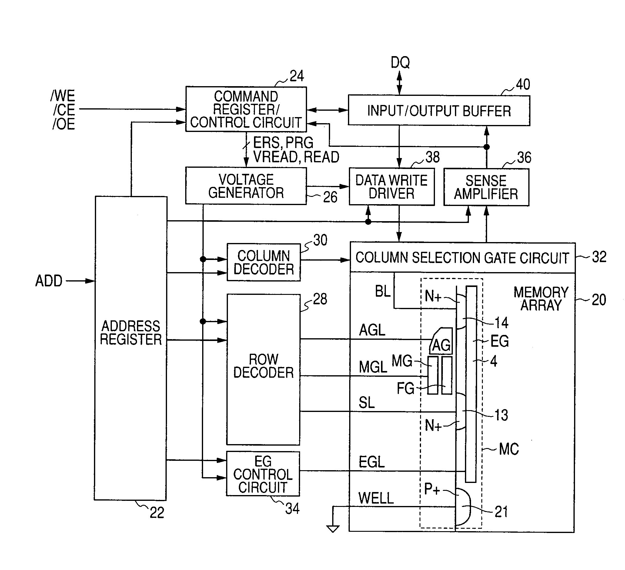
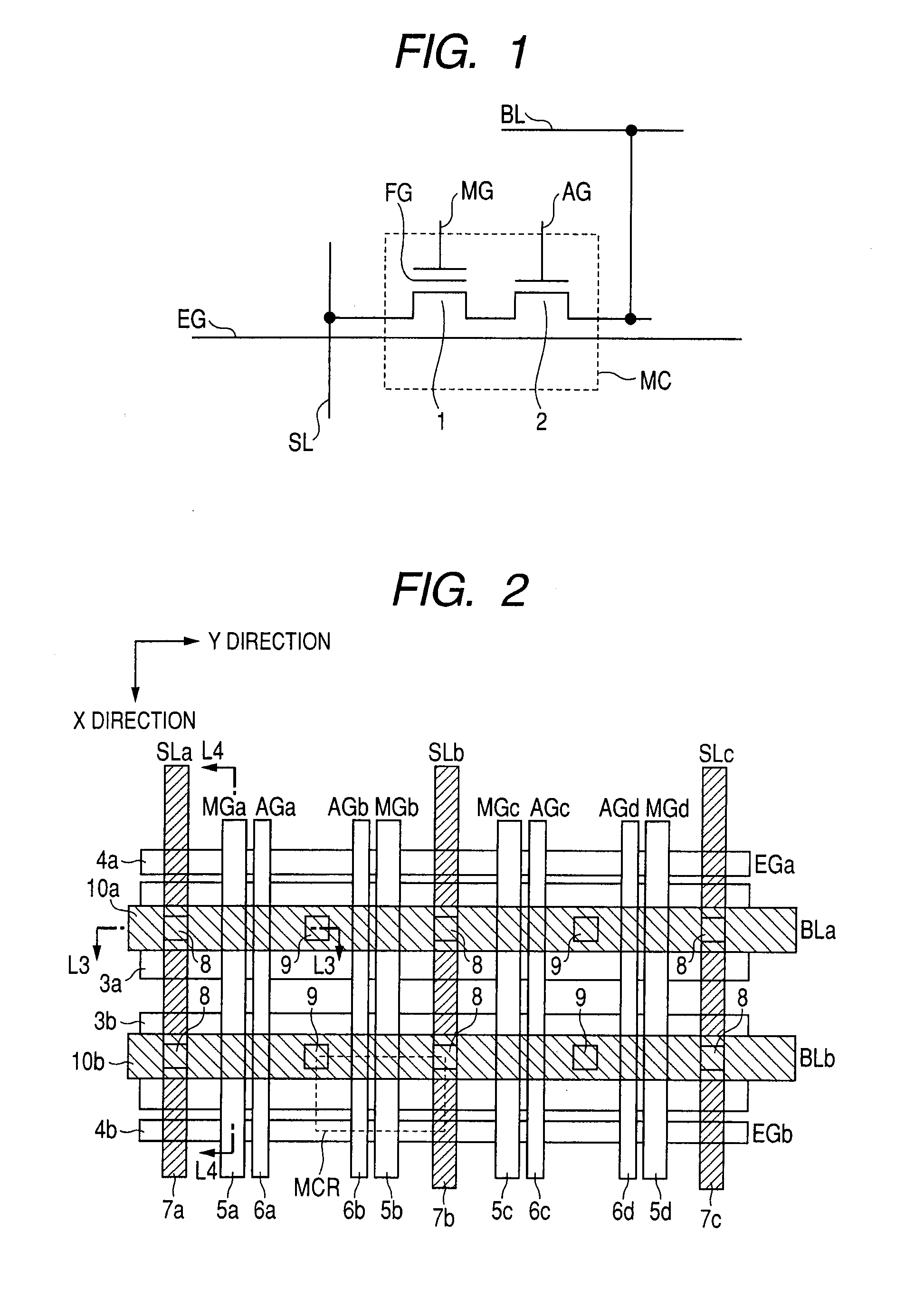
[0107]FIG. 1 is a diagram schematically showing an electrical equivalent circuit of a memory cell in a semiconductor device employed in the first embodiment of the present invention. In FIG. 1, the memory cell MC includes a memory transistor 1 having a floating gate FG, and an assist gate transistor (selection transistor) 2 coupled in series with the memory transistor 1. The memory transistor 1 is of an N channel MOS transistor (insulated gate field effect transistor) having a stacked gate structure of a floating gate FG and a memory gate MG formed in its upper layer and has a source impurity region coupled to a source line SL. The assist gate transistor 2 is of an N channel MOS transistor of a single layer gate structure having an assist gate AG and has an impurity region coupled to a bit line BL. An impurity region is not formed between these assist gate transistor 2 and memory gate transistor 1.

[0108]The memory cell MC further has an erase gate EG. The erase gate EG is formed in ...

second embodiment

[0170]FIG. 14 is a diagram schematically showing an overall configuration of a semiconductor device according to a second embodiment of the present invention. The semiconductor device shown in FIG. 14 is different in configuration from the semiconductor device shown in FIG. 9 in the following points. Namely, as for a memory array 20, it is divided into a plurality of column blocks by a plurality of embedded erase gate lines EGLA and EGLB. The embedded erase gate line EGLA (EG (0)) is coupled to an embedded erase gate EG of a memory cell MCa, and the embedded erase gate line EGLB (EG (1)) is coupled to an embedded erase gate EG of a memory cell MCb. The memory cells MCa and MCb are respectively coupled to bit lines BL (0) and BL (1).

[0171]The memory array 20 has a single bank structure and is not capable of performing data access to each memory cell of another row in parallel upon data access to each memory cell of a given row (reading from or writing to the memory cell).

[0172]An EG ...

third embodiment

[0197]FIG. 20 is a diagram schematically showing voltages applied to a memory cell where erasure and reading are performed in parallel. In FIG. 20, an erase high voltage Veg (=10V) is applied to an embedded erase gate EG upon the erasure. Upon the reading, a read voltage Vag (=1.5V) is applied to an assist gate AG. Upon the reading, a read voltage (1.0V) is applied to a bit line BL. In this state, a channel 60 is formed in a substrate region surface adjacent to a drain impurity region 14 by the voltage Vag on the assist gate AG upon the reading. In this state, a parasitic capacitance C0 exists between the embedded erase gate EG and a floating agate FG. A parasitic capacitance C1 exists between the floating gate FG and the assist gate AG. A parasitic capacitance C2 exists even between the floating gate FG and the channel 60.

[0198]Upon the normal erase operation similar to the conventional one, the assist gate AG and the bit line BL are in an open state or 0V (ground voltage), and the...


PUM


Abstract

The present invention provides a semiconductor device having a nonvolatile memory function capable of shortening an erase time and executing data access efficiently. When, under the control of a command register/control circuit, an erase voltage is applied to an embedded erase gate wiring disposed in a memory cell boundary region, and an electrical charge is transferred between a floating gate and an embedded erase gate to thereby perform an erase operation, a read selection voltage is applied to a memory gate line and an assist gate line during the application of the erase voltage to thereby carry out the reading of data.

Description

CROSS-REFERENCE TO RELATED APPLICATIONS[0001]The disclosure of Japanese Patent Application No. 2009-119016 filed on May 15, 2009 including the specification, drawings and abstract is incorporated herein by reference in its entirety.BACKGROUND OF THE INVENTION[0002]The present invention relates to a semiconductor device having the function of storing information therein on a non-volatile basis, and particularly to a semiconductor device having nonvolatile memory cells each storing information therein on a non-volatile basis according to the amount of an electrical charge accumulated in a charge storage layer such as a floating gate. More specifically, the present invention relates to a configuration for performing data access in parallel during an erase operation mode.[0003]A flash memory is of a memory which stores information therein on a non-volatile basis. The flash memory has been widely used for the storage of boot program information to a processor and the storage of an applic...

Claims


Application Information

Patent Timeline
IPC IPC(8): G11C16/06G11C16/04
CPCG11C16/10G11C16/344G11C16/3445G11C16/16G11C16/3459G11C2216/22G11C16/3454
Inventor TANIZAKI, HIROAKIKUNORI, YUICHIFUTATSUYA, TOMOSHIKODA, KENJI
Owner RENESAS ELECTRONICS CORP
Why Eureka
Try Eureka