Bump printing apparatus and method of controlling the same

a printing apparatus and printing method technology, applied in resistive material coating, non-electric welding apparatus,auxillary welding devices, etc., can solve the problems of mask sag, reduce the printability of bumps, and the speed at which masks and boards are separated varies according to the speed, so as to increase the printability of solder bumps, prevent the generation of bump defects, and increase the reliability of boards

Inactive Publication Date: 2010-11-18
SAMSUNG ELECTRO MECHANICS CO LTD
View PDF9 Cites 14 Cited by
  • Summary
  • Abstract
  • Description
  • Claims
  • Application Information

AI Technical Summary

Benefits of technology

[0013]An aspect of the present invention provides a bump printing apparatus and a method of controlling the same that can increase the printability of solder bumps by allowing for the easy withdrawal of solder pastes so as to maintain the shapes of bumps and increase the reliability of a board by preventing the generation of bump defects.

Problems solved by technology

However, according to these methods, when the mask and the PCB are forcibly separated from each other, the mask sags and thus the speeds at which the mask and the board are separated vary according to portions.
Therefore, bump defects, such as the spreading of solder pastes, short circuits and missing bumps, in which bumps are not formed, occur to reduce the printability of bumps, which may reduce the reliability of printed circuit boards.

Method used


Image

  • Bump printing apparatus and method of controlling the same
  • Bump printing apparatus and method of controlling the same
  • Bump printing apparatus and method of controlling the same

Examples


Embodiment Construction

[0036]Exemplary embodiments of the present invention will now be described in detail with reference to the accompanying drawings.

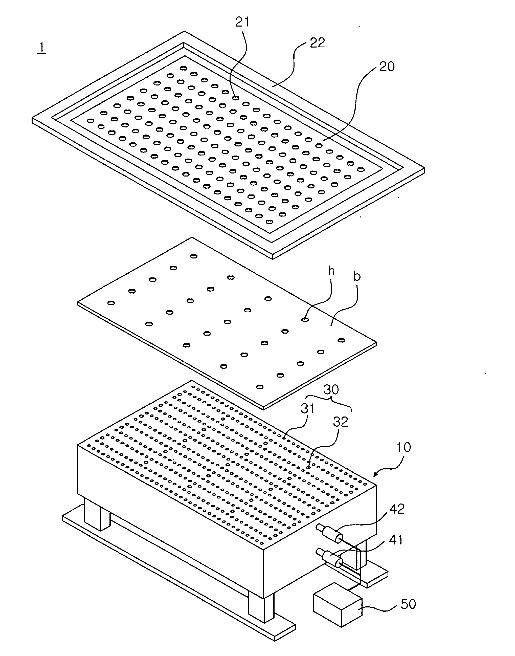
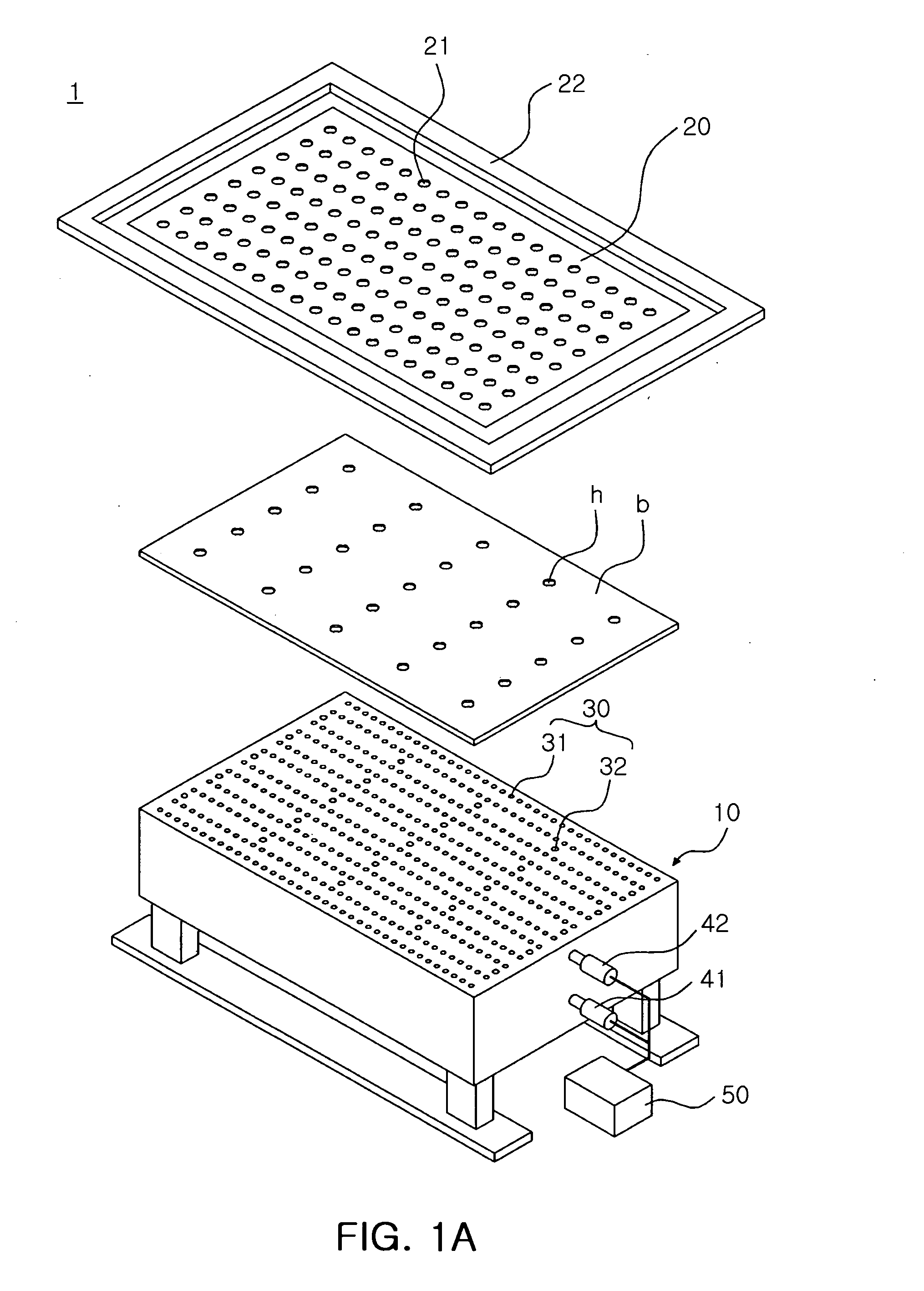
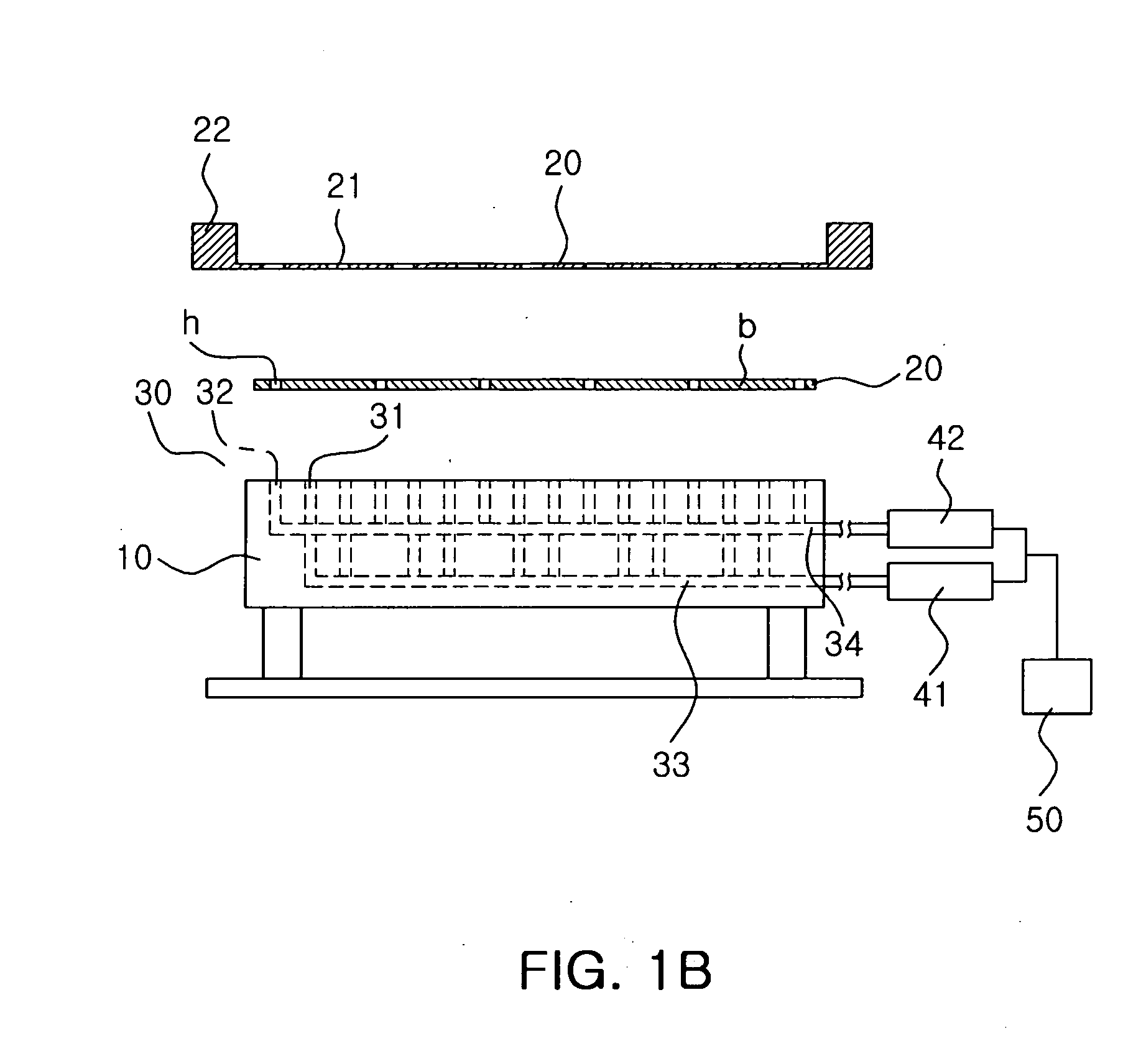
[0037]FIG. 1A is a perspective view schematically illustrating a bump printing apparatus according to an exemplary embodiment of the invention. FIG. 1B is a cross-sectional view schematically illustrating the bump printing apparatus shown in FIG. 1A. FIG. 2 is a plan view illustrating a printing table including suction nozzles and spray nozzles of the bump printing apparatus, shown in FIGS. 1A and 1B. FIG. 3 is a cross-sectional view illustrating the printing table, shown in FIG. 2.

[0038]FIG. 4A is a cross-sectional view schematically illustrating another example of the spray nozzles of the printing table, shown in FIG. 3. FIG. 4B is a plan view schematically illustrating another example of the spray nozzles of the printing table, shown in FIG. 3. FIG. 5A is a cross-sectional view schematically illustrating another example of the spray nozzles of the print...


PUM

PropertyMeasurementUnit
air pressureaaaaaaaaaa
air suctionaaaaaaaaaa
conductivityaaaaaaaaaa

Abstract

There is provided a bump printing apparatus and a method of controlling the same that can increase the printability of solder bumps being printed on a board. The bump printing apparatus may include a printing table onto which a board is mounted; a mask making close contact with the board and printing solder bumps on the board by separating the mask from the board after a printing operation; and air nozzles provided within the printing table and providing air suction to bring the board into close contact with the printing table and spraying air to separate the mask from the board.

Description

CROSS-REFERENCE TO RELATED APPLICATIONS[0001]This application claims the priority of Korean Patent Application No. 10-2009-0041644 filed on May 13, 2009, in the Korean Intellectual Property Office, the disclosure of which is incorporated herein by reference.BACKGROUND OF THE INVENTION[0002]1. Field of the Invention[0003]The present invention relates to a bump printing apparatus and a method of controlling the same, and more particularly, to a bump printing apparatus and a method of controlling the same that can increase the printability of solder bumps being printed on a board.[0004]2. Description of the Related Art[0005]In general, flip chip bonding, tape automated bonding and wire bonding are being used to interconnect external boards, such as printed circuit boards (PCBs) or wafer level packages (WLPs), to chips.[0006]Among them, flip chip bonding has been widely used to manufacture portable electronic products, since this method increases the number of pads per unit area.[0007]A...

Claims


Application Information

Patent Timeline
Patent Type & Authority Applications(United States)
IPC IPC(8): B05D5/12B05C5/00
CPCH05K3/1233H05K3/3484H05K2201/09063H05K2203/082H05K2203/0264H05K2203/043H05K2203/081H05K2203/0165H05K3/3485
Inventor KIM, JOON KON
Owner SAMSUNG ELECTRO MECHANICS CO LTD
Why Eureka
Try Eureka