Method and system for detailed placement of layout objects in a standard-cell layout design

a layout design and layout object technology, applied in the field of standard-cell layout designs, can solve the problems of small focus/process window depth, poor lithographic response, unwanted printing of srafs on the wafer, etc., and achieve the effect of reducing cd errors

Inactive Publication Date: 2007-07-19
RPX CORP
View PDF18 Cites 39 Cited by
  • Summary
  • Abstract
  • Description
  • Claims
  • Application Information

AI Technical Summary

Benefits of technology

[0015] The system includes a placement perturbation module and a standard-cell layout generator. The placement perturbation module calculates the layout perturbation distanc

Problems solved by technology

When off-axis illumination is optimized for one pitch (usually the minimum or the most commonly used pitch in the design), there will always be other pitches for which angle of illumination and angle of diffraction together lead to a poor lithographic response and hence a small depth of focus/process window.
Incorrect placement of SRAFs can result in unwanted printing of SRAFs on the wafer.
At the same time, large spacing can make the SRAFs less effective in helping with printability.
In etch processes, different consumptions of etchants with different pattern density lead to etch skew between den

Method used


Image

  • Method and system for detailed placement of layout objects in a standard-cell layout design
  • Method and system for detailed placement of layout objects in a standard-cell layout design
  • Method and system for detailed placement of layout objects in a standard-cell layout design

Examples


Embodiment Construction

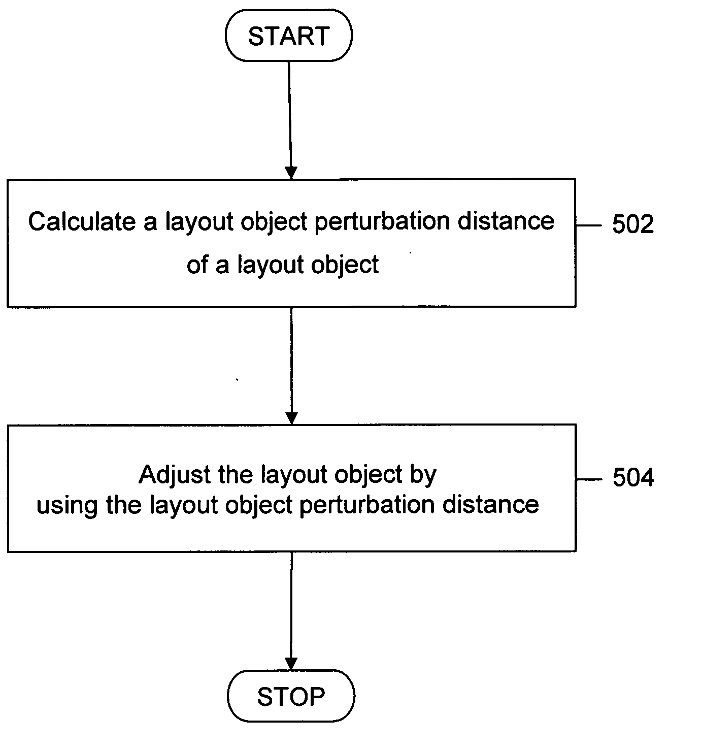
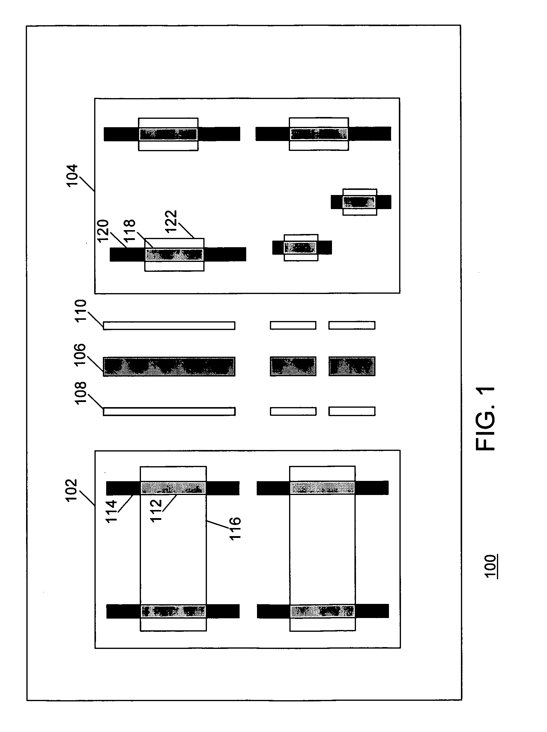
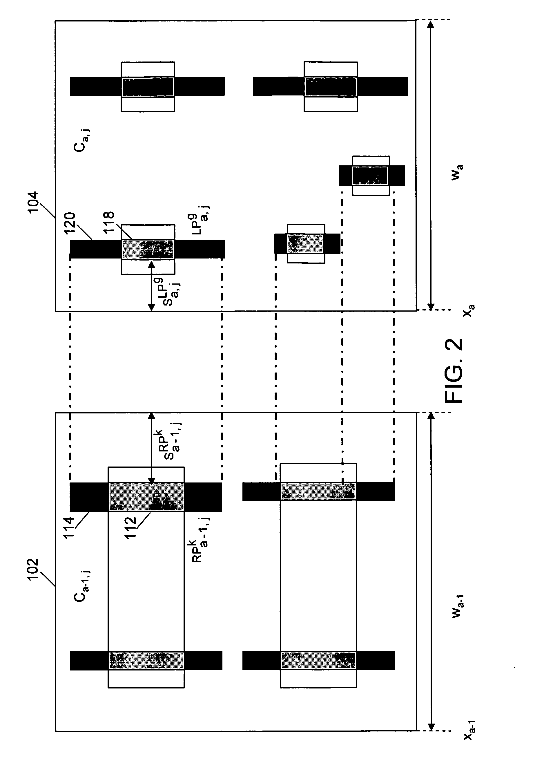
[0027] Various embodiments of the present invention relate to a method and system for detailed placement of layout objects in a standard-cell layout design. A standard-cell layout generated in accordance with various embodiments of the present invention can be used to prepare a photolithography mask that offers improved lithographic characteristics. The lithographic mask can then be used to manufacture an integrated circuit. Layout objects are design objects that need to be positioned in a standard-cell layout design according to specific rules. Layout objects include traditional design objects such as cells. Typically, placement of a cell is chosen by a physical design tool. Exemplary physical design tools include Astro™ from Synopsys and SOC Encounter™ from Cadence. Each cell can further include a plurality of polysilicon shapes and their active-layer shapes. Each of the plurality of polysilicon shapes can include a plurality of gate polysilicon shapes (that is to say, transistor ...


PUM


Abstract

A method and system for detailed placement of layout objects in a standard-cell layout design are disclosed. Layout objects comprise cells and etch dummies. The method includes a programming based technique to calculate layout object perturbation distances for the layout objects. The method includes adjusting the layout objects with their corresponding layout object perturbation distances. This leads to improved photolithographic characteristics such as reduced Critical Dimension (CD) errors and forbidden pitches in the standard-cell layout.

Description

BACKGROUND OF THE INVENTION [0001] 1. Field of the Invention [0002] This invention relates generally to standard-cell layout designs, and more particularly, to a dynamic system and method for adjustment of the placement of layout objects, such as the cells and etch dummies used with standard-cell layout designs. [0003] 2. Description of the Related Art [0004] The feature size of modern standard cell-based layout designs of integrated circuits has reached nanometer scale. For example, the feature size of leading optical lithographic processes is significantly smaller than that of the wavelength of the light used, resulting in a “sub-wavelength lithography” regime. This requires advanced photomasks that embody one or more resolution enhancement techniques (RETs) such as optical proximity correction (OPC), phase shift masks (PSM), off-axis illumination (OAI), and the insertion of sub-resolution assist features (SRAFs). These techniques achieve enhanced critical dimension (CD) control i...

Claims


Application Information

Patent Timeline
IPC IPC(8): G06F17/50
CPCG06F17/5068G06F30/39
Inventor GUPTA, PUNEETKAHNG, ANDREW B.PARK, CHUL-HONG
Owner RPX CORP
Why Eureka
Try Eureka