Nanowire photodetector and image sensor with internal gain

a photodetector and nanowire technology, applied in the field of photodetectors and image sensors, can solve the problems of difficult incorporation of nanowires as photodetectors in practical cmos integration, sensor fixed pattern and dark-current noise, etc., and achieve the effect of enhancing the photocurrent response and high gain

Inactive Publication Date: 2010-11-25
RGT UNIV OF CALIFORNIA
View PDF10 Cites 70 Cited by
  • Summary
  • Abstract
  • Description
  • Claims
  • Application Information

AI Technical Summary

Benefits of technology

[0015]The invention provides a practical 1D nanowire photodetector with high gain that can be controlled by a radial electric field established in the 1D nanowire. A 1D nanowire photodetector device in embodiments of the invention includes a nanowire that is individually contacted by electrodes for applying a longitudinal electric field that drives the photocurrent. An intrinsic electric field in the radial direction of the nanowire inhibits photo-carrier recombination, thus enhancing the photocurrent response. The invention further provides circuits of 1D nanowire photodetectors, with groups of photodetectors ad

Problems solved by technology

CMOS image sensors are more likely than CCD images sensors to suffer from fixed-pattern and dark-current noise.
However, the incorporation of nanowires as photodetectors in practical CMOS integrations has proven difficult.
Additionally, the photon absorption, gain and current generation in nanowires are not fully understood.
Another issue in making practical use of nanowires as photodetectors involves the placement of nanowires and connecting into integrated circuits.
While nanowires have been used in groups to realize photodetection and can be deposited in parallel by the standard Langmuir-Blodgett technique for this purpose, the registered placement and registration of nanowires n

Method used


Image

  • Nanowire photodetector and image sensor with internal gain
  • Nanowire photodetector and image sensor with internal gain
  • Nanowire photodetector and image sensor with internal gain

Examples


Embodiment Construction

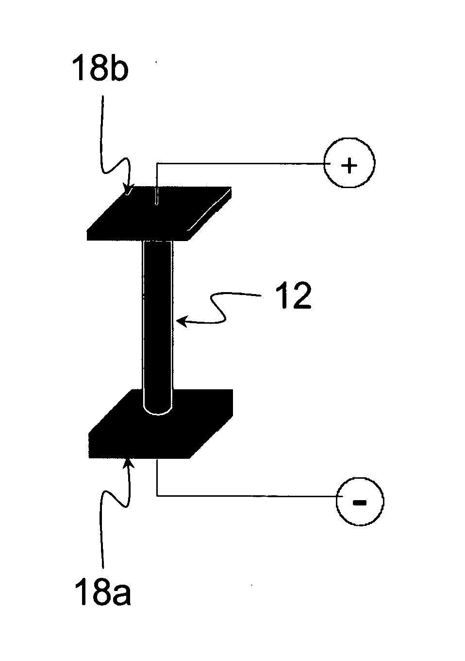
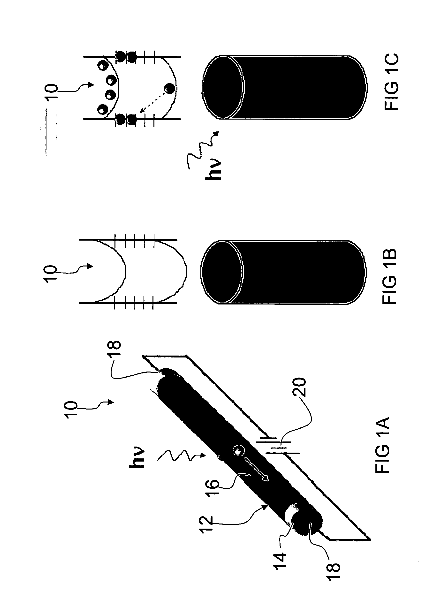
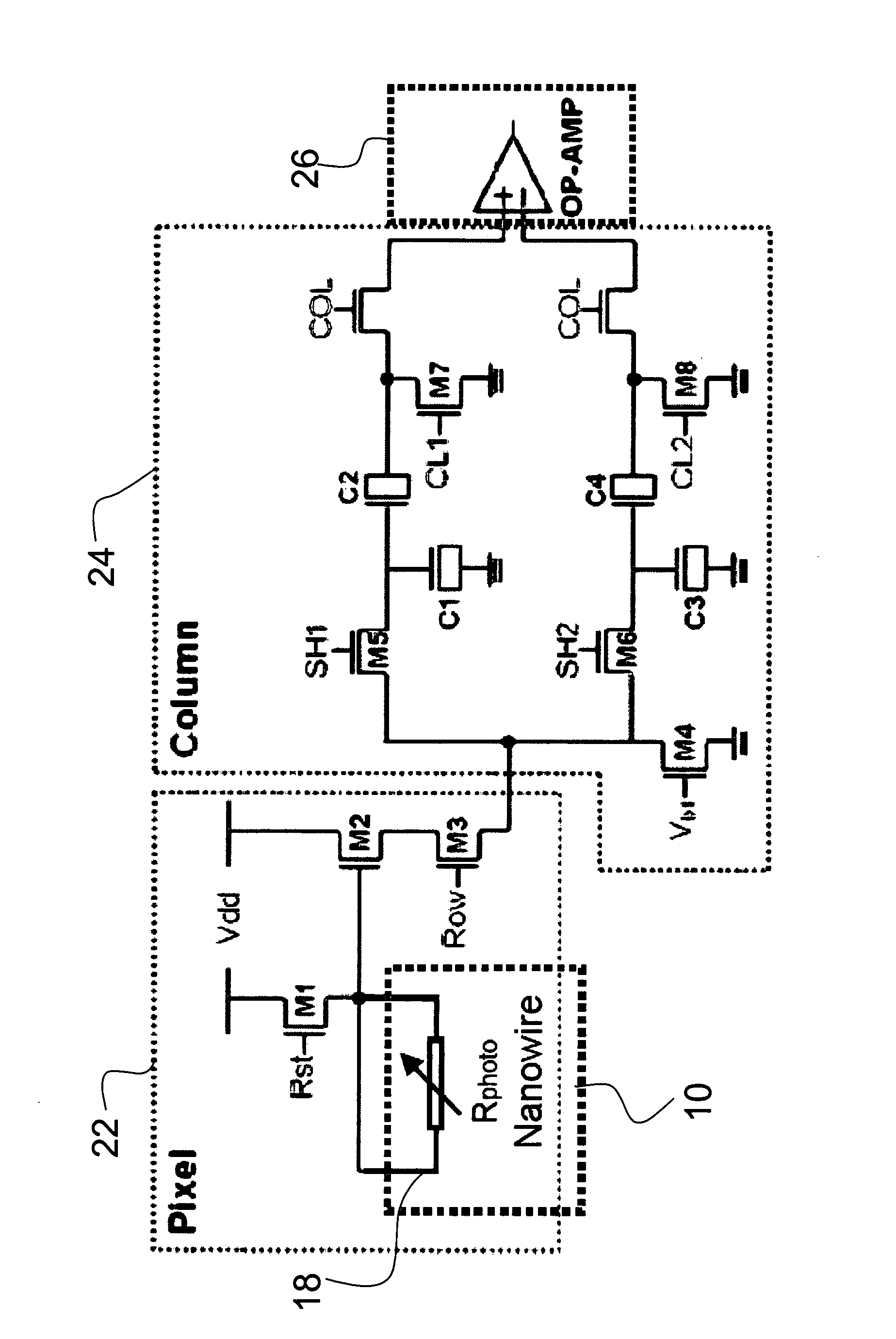
[0022]The invention provides a practical 1D nanowire photodetector with high gain that can be controlled by a radial electric field established in the 1D nanowire. A 1D nanowire photodetector device of the invention includes a nanowire that is individually contacted by electrodes for applying a longitudinal electric field which drives the photocurrent. An intrinsic radial electric field to the nanowire inhibits photo-carrier recombination, thus enhancing the photocurrent response. The invention further provides circuits of 1D nanowire photodetectors, with groups of photodetectors addressed by their individual 1D nanowires electrode contacts.

[0023]1D nanowire photodetectors with internal gain of the invention can be realized with different materials, including group IV, III-V, II-VI semiconductors. A preferred 1D nanowire photodetector is a ZnO nanowire with a radial doping profile that inhibits hole and electron recombination. Embodiments of the invention provide the ability to inte...


PUM


Abstract

A practical ID nanowire photodetector with high gain that can be controlled by a radial electric field established in the ID nanowire. A ID nanowire photodetector device of the invention includes a nanowire that is individually contacted by electrodes for applying a longitudinal electric field which drives the photocurrent. An intrinsic radial electric field to the nanowire inhibits photo-carrier recombination, thus enhancing the photocurrent response. The invention further provides circuits of ID nanowire photodetectors, with groups of photodetectors addressed by their individual ID nanowires electrode contacts. The invention also provides a method for placement of ID nanostructures, including nanowires, with registration onto a substrate. A substrate is patterned with a material, e.g., photoresist, and trenches are formed in the patterning material at predetermined locations for the placement of ID nanostructures. The ID nanostructures are aligned in a liquid suspension, and then transferred into the trenches from the liquid suspension. Removal of the patterning material places the ID nanostructures in predetermined, registered positions on the substrate.

Description

PRIORITY CLAIM AND REFERENCE TO RELATED APPLICATION[0001]This application claims priority under 35 U.S.C. §119 from prior provisional application Ser. No. 60 / 903,633, which was filed on Feb. 27, 2007; and from prior provisional application Ser. No. 60 / 903,750, which was filed on Feb. 27, 2007.STATEMENT OF GOVERNMENT INTEREST[0002]This application was made with Government support under National Science Foundation Contract No. ECS-0506902 and Office of Naval Research Contract No. N00014-05-1-0149. The Government has certain rights in this invention.FIELD[0003]A field of the invention is photodetection and image sensing. The invention concerns photodetector and image sensors that convert optical signals into electrical signals.BACKGROUND[0004]Any electronic device that detects and / or processes optical signals must convert the sensed signals to electrical signals. This is accomplished with a photodetector. Image sensors include a spatial arrangement of photodetectors (pixels) that can b...

Claims


Application Information

Patent Timeline
IPC IPC(8): H01L27/146H01L31/18
CPCH01L27/14643B82Y20/00H01L31/035236H01L31/035227
Inventor WANG, DELISOCI, CESARELO, YU-HWAZHANG, ARTHURAPLIN, DAVIDWANG, LINGQUANDAYEH, SHADIBAO, XIN YU
Owner RGT UNIV OF CALIFORNIA
Why Eureka
Try Eureka