Manufacture of light emitting devices with phosphor wavelength conversion

a technology of light emitting devices and manufacturing methods, applied in the direction of semiconductor/solid-state device manufacturing, semiconductor devices, electrical equipment, etc., can solve the problems of color/cct variation compounding, color/cct variation can become a significant problem, and the method of manufacture is cost, so as to reduce or eliminate the need for binning packaged devices

Inactive Publication Date: 2010-11-25
INTEMATIX
View PDF26 Cites 50 Cited by
  • Summary
  • Abstract
  • Description
  • Claims
  • Application Information

AI Technical Summary

Benefits of technology

[0029]The present invention arose in an endeavor to address, at least in part, the problem of color hue and/or CCT variation of l...

Problems solved by technology

A drawback with such a method of manufacture is cost, since phosphor has to be applied to the LED chip on an individual basis.
The problem of color/CCT variation is compounded by the fact that the human eye is extremely sensitive to subtle changes in color hue especially in the white color range.
Furthermore, in applications in which the device includes further optical components, in particular a lens, to focus the output light, such color/CCT variation can become a significant problem.
In addition to the problem of non-uniformity in emitted color/CCT due to the variation in path length through the phosphor/polymer encapsulation, it is found that the phosphor material(s) can accumulate unevenly during curing of the liquid polymer resulting in a non-uniform distribution of the phosphor material(s) over the LED chip and in pa...

Method used


Image

  • Manufacture of light emitting devices with phosphor wavelength conversion
  • Manufacture of light emitting devices with phosphor wavelength conversion
  • Manufacture of light emitting devices with phosphor wavelength conversion

Examples


Embodiment Construction

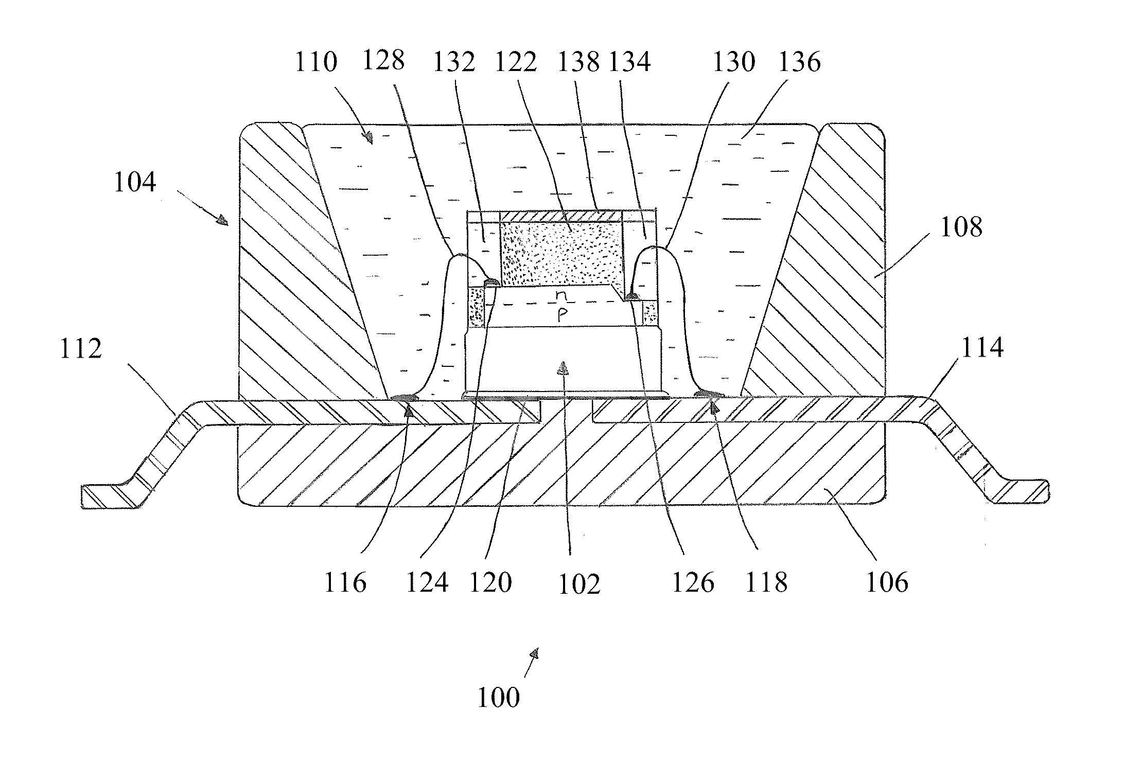
[0047]Embodiments of the invention concern methods of manufacturing a light emitting device with phosphor wavelength conversion and in particular methods of applying / processing the phosphor material on an LED wafer prior to division of the wafer into individual LED chips. More particularly the method concerns patterning of the phosphor material to enable electrical connections to be made to the LED chip's electrode contacts once the wafer is subsequently divided into individual LED chips. The term “LED wafer” refers to a wafer (substrate) on which the LED chips are fabricated by depositing layers of n-type and p-type semiconductor materials. This is to be contrasted with a wafer (substrate) onto which individual LED chips are mounted post fabrication.

[0048]In this specification like reference numerals are used to denote like parts. FIG. 3 is a schematic sectional view of a white light emitting device 100 with phosphor wavelength conversion in accordance with the invention. The devic...


PUM


Abstract

A method of manufacturing a light emitting device comprises: depositing over substantially the entire surface of a LED wafer having a array of LEDs formed on a surface thereof a mixture of at least one phosphor and a polymer material, wherein the polymer material is transmissive to light generated by the LEDs and to light generated by the at least one phosphor material; using laser ablation to selectively make apertures in the phosphor/polymer material corresponding to electrode contact pads of each LED thereby enabling access to each electrode contact pad; and dividing the wafer into individual light emitting devices. The method can further comprise, prior to dividing the wafer, cutting slots in the phosphor/polymer material which are configured to pass between individual LEDs. The slots are configured such that a layer of phosphor/polymer material remains on the edges of each LED after division of the wafer into individual light emitting devices.

Description

CROSS-REFERENCE TO RELATED APPLICATIONS[0001]This application claims the benefit of priority of U.S. Provisional Application No. 61 / 179,671, filed May 19, 2009, the contents of which are incorporated herein by reference.BACKGROUND OF THE INVENTION[0002]1. Field of the Invention[0003]The invention relates to methods of manufacture of light emitting devices with phosphor wavelength conversion. More particularly the invention concerns a method of applying a phosphor material to a light emitting diode (LED).[0004]2. Description of the Related Art[0005]White light emitting LEDs (“white LEDs”) are known in the art and are a relatively recent innovation. It was not until LEDs emitting in the blue / ultraviolet part of the electromagnetic spectrum were developed that it became practical to develop white light sources based on LEDs. As taught, for example in U.S. Pat. No. 5,998,925, white LEDs include one or more phosphor materials, that is photo-luminescent materials, which absorb a portion o...

Claims


Application Information

Patent Timeline
IPC IPC(8): H01L33/50H01L21/50
CPCH01L33/0095H01L33/50H01L33/54H01L33/62H01L2933/0041H01L2933/0066H01L2924/01322H01L2224/48247H01L2224/48465H01L2224/49107H01L2224/73265H01L2224/8592H01L2224/32245H01L2224/48091H01L2924/00014H01L2924/00H01L2924/181H01L2924/00012
Inventor MELMAN, JONATHAN
Owner INTEMATIX
Why Eureka
Try Eureka