Method of forming a planar field effect transistor with embedded and faceted source/drain stressors on a silicon-on-insulator (SOI) wafer, a planar field effect transistor structure and a design structure for the planar field effect transistor

a technology of source/drain stressor and planar field effect, which is applied in the field of planar field effect transistors, can solve the problems of incompatibility of the technique with the silicon-on-insulator (soi) wafer, incompatible with the current state of the art thin soi, wafers and ultra-thin soi, etc., and achieve the effect of increasing the depth of the recesses

Active Publication Date: 2010-11-25
GLOBALFOUNDRIES US INC
View PDF2 Cites 70 Cited by
  • Summary
  • Abstract
  • Description
  • Claims
  • Application Information

AI Technical Summary

Benefits of technology

[0006]In view of the foregoing, disclosed herein are embodiments of a method of forming, on a silicon-on-insulator (SOI) wafer, a planar field effect transistor (FETs) with embedded and faceted source/drain stressors. The method embodiments can incorporate a directional ion implant process to create amorphous regions at the bottom surfaces of source/drain recesses in a single crystalline semiconductor layer of an SOI wafer. Then, an etch process selective to different crystalline planes over others and further selective to single crystalline semiconductor material over amorphous semiconductor material can be performed in order to selectively ad

Problems solved by technology

Unfortunately, this technique is incompatible with silicon-on-insulator (SOI) wafers and, more particularly, incompatib

Method used


Image

  • Method of forming a planar field effect transistor with embedded and faceted source/drain stressors on a silicon-on-insulator (SOI) wafer, a planar field effect transistor structure and a design structure for the planar field effect transistor
  • Method of forming a planar field effect transistor with embedded and faceted source/drain stressors on a silicon-on-insulator (SOI) wafer, a planar field effect transistor structure and a design structure for the planar field effect transistor
  • Method of forming a planar field effect transistor with embedded and faceted source/drain stressors on a silicon-on-insulator (SOI) wafer, a planar field effect transistor structure and a design structure for the planar field effect transistor

Examples


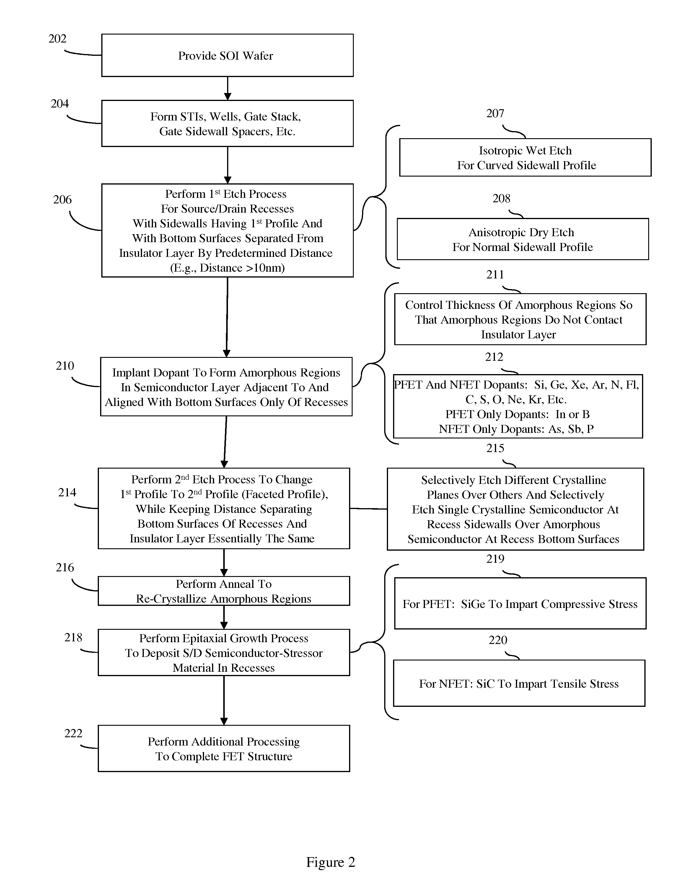
Embodiment Construction

[0024]The embodiments of the invention and the various features and advantageous details thereof are explained more fully with reference to the non-limiting embodiments that are illustrated in the accompanying drawings and detailed in the following description.

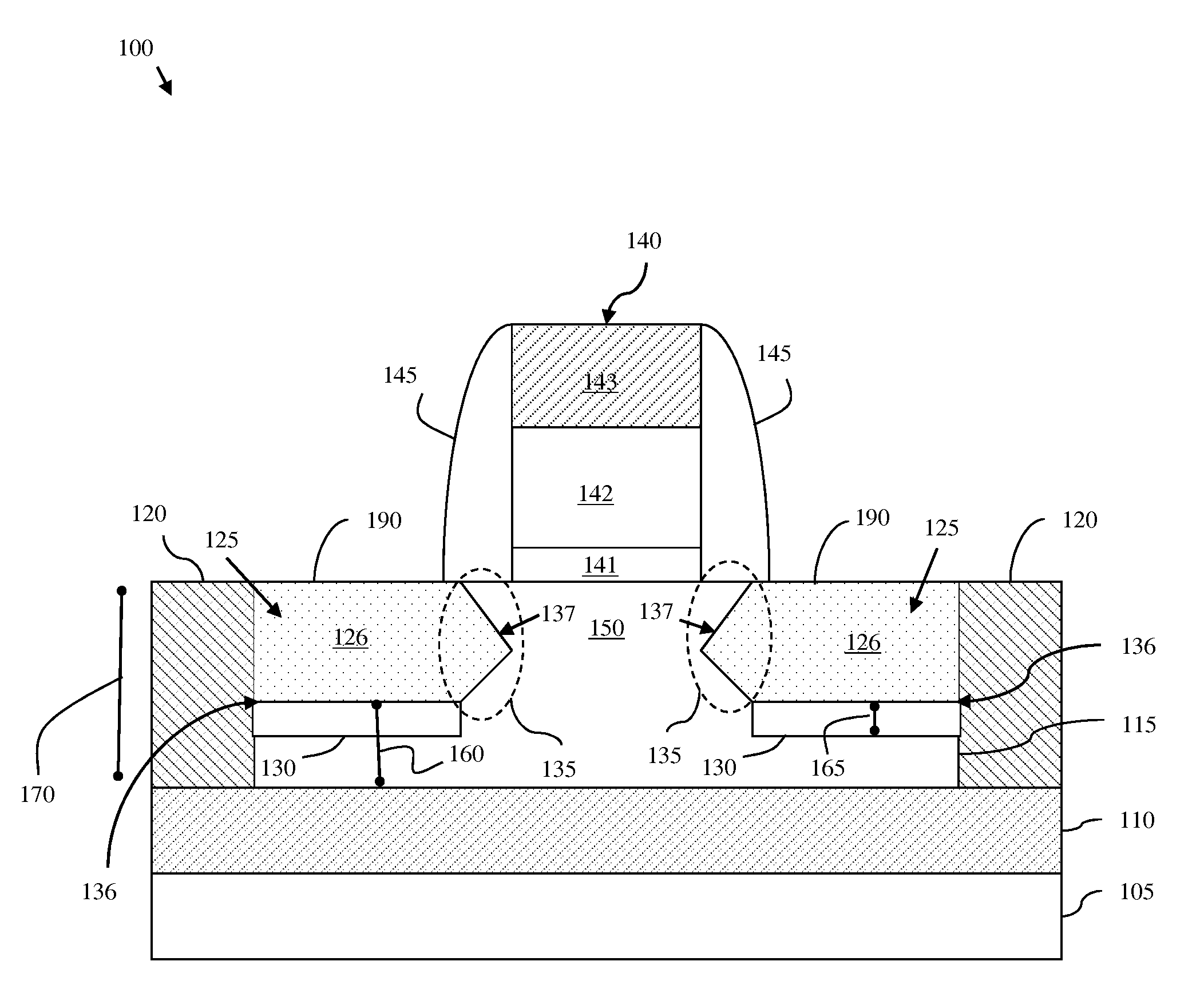
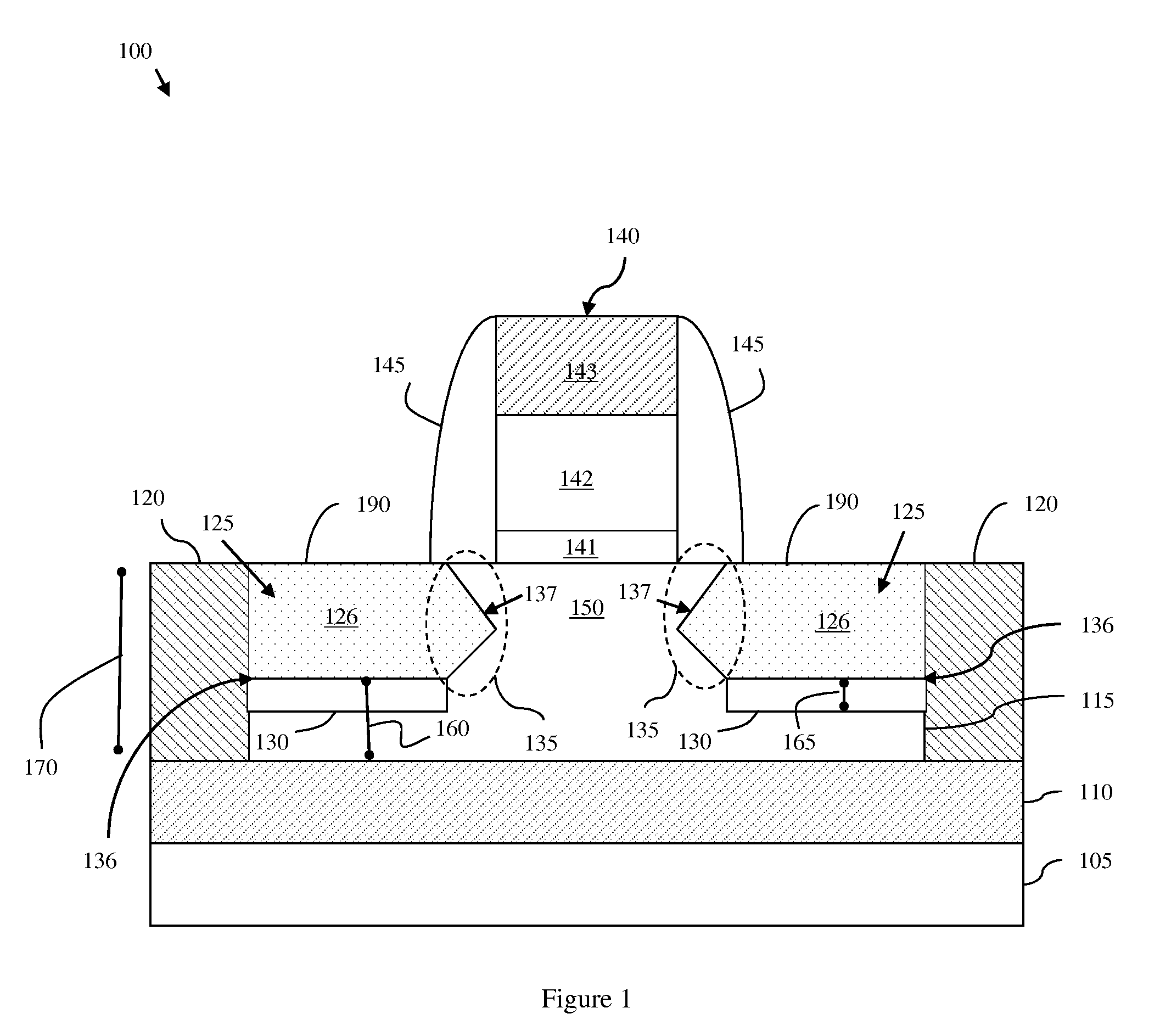
[0025]As mentioned above, charge carrier mobility impacts current flowing through the channel region of field effect transistors (FETs). That is, in n-type field effect transistors (NFETS) current flow is proportional to the mobility of electrons in the channel region, whereas in p-type field effect transistors (PFETs) current flow is proportional to the mobility of holes in that channel region. Stress can be imposed upon on the channel region in order to adjust carrier mobility and, thereby, adjust current flow. Specifically, compressive stress on the channel region of a PFET can enhance hole mobility and, thereby increase drive current. Contrarily, tensile stress on the channel region of an NFET can enhance electron mobility...


PUM


Abstract

Disclosed are embodiments of a method of forming, on an SOI wafer, a planar FET with embedded and faceted source/drain stressors. The method incorporates a directional ion implant process to create amorphous regions at the bottom surfaces of source/drain recesses in a single crystalline semiconductor layer of an SOI wafer. Then, an etch process selective to different crystalline planes over others and further selective to single crystalline semiconductor material over amorphous semiconductor material can be performed in order to selectively adjust the shape (i.e., the profile) of the recess sidewalls without increasing the depth of the recesses. Subsequently, an anneal process can be performed to re-crystallize the amorphous regions and an epitaxial deposition process can be used to fill the recesses with source/drain stressor material. Also disclosed are embodiments of a planar FET structure and a design structure for the planar FET.

Description

BACKGROUND[0001]1. Field of the Invention[0002]The embodiments of the invention generally relate to planar field effect transistors (FETs) and, more particularly, to a method of forming a planar FET with embedded and faceted source / drain stressors on a silicon-on-insulator (SOI) wafer, a planar FET structure and a design structure for the planar FET.[0003]2. Description of the Related Art[0004]Charge carrier mobility impacts current flowing through the channel region of field effect transistors (FETs). That is, in n-type field effect transistors (NFETS) current flow is proportional to the mobility of electrons in the channel region, whereas in p-type field effect transistors (PFETs) current flow is proportional to the mobility of holes in that channel region. Stress can be imposed upon on the channel region in order to adjust carrier mobility and, thereby, adjust current flow. Specifically, compressive stress on the channel region of a PFET can enhance hole mobility and, thereby inc...

Claims


Application Information

Patent Timeline
IPC IPC(8): H01L29/786H01L21/336G06F17/50
CPCH01L21/26506H01L29/1079H01L29/78654H01L29/66772H01L29/7848H01L29/66636H01L21/26566
Inventor CHENG, KANGGUOFALTERMEIER, JOHNATHAN E.FURUKAWA, TOSHIHARUHUA, XUEFENG
Owner GLOBALFOUNDRIES US INC
Why Eureka
Try Eureka