

Two-dimensional solid-state imaging device
a solid-state imaging and two-dimensional technology, applied in the field of two-dimensional solid-state imaging devices, can solve the problems of insufficient reproducibility of color information, insufficient description of a specific polarization component detection technique, and insufficient description of specified two-dimensional pixel arrangement for realizing a two-dimensional solid-state imaging element, so as to increase the degree of freedom for signal wiring, reduce the opening area of the photoelectric conversion element, and reduce the number of pixels per unit area
- Summary
- Abstract
- Description
- Claims
- Application Information
AI Technical Summary
Benefits of technology
Problems solved by technology
Method used
Image

Examples
example 1
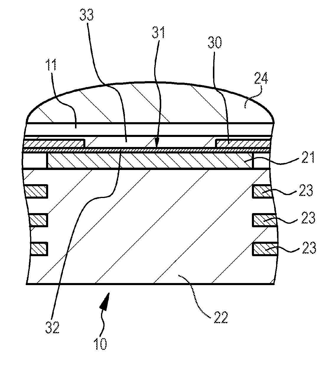
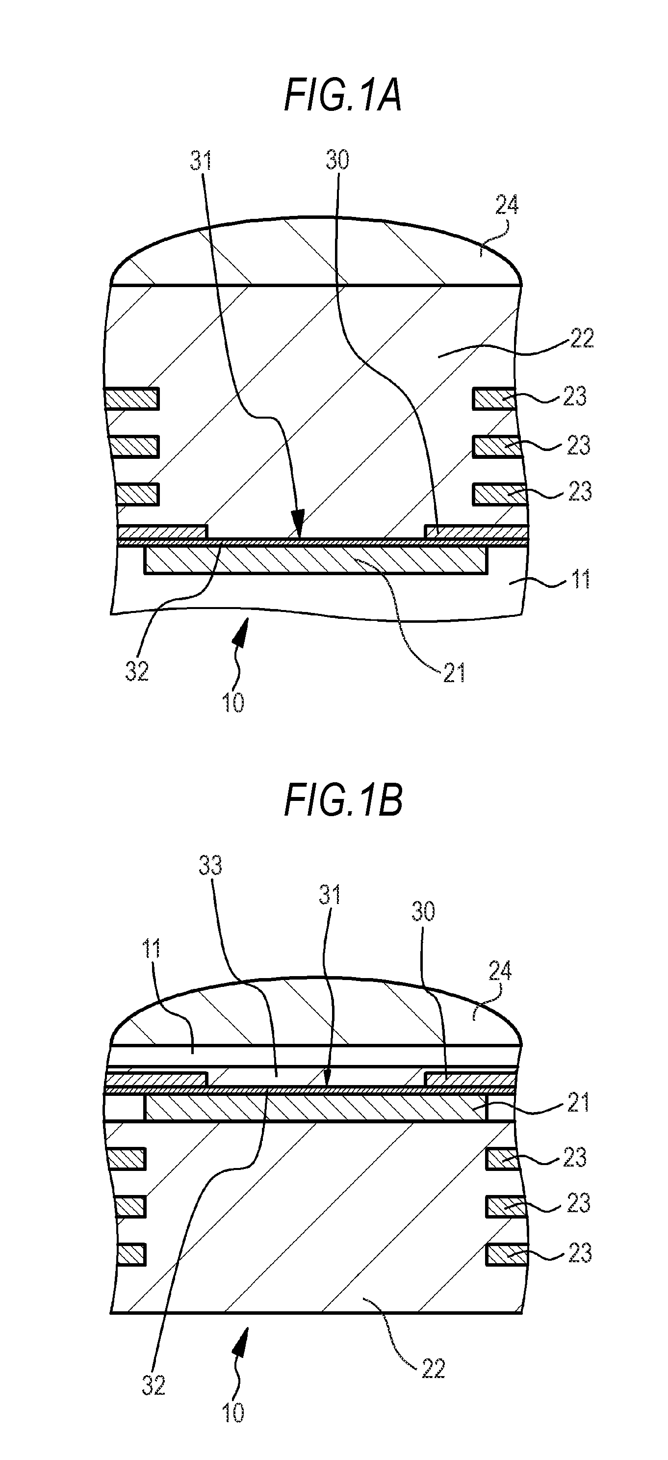
[0075]Example 1 relates to the two-dimensional solid-state imaging device according to the first embodiment of the invention, and to a two-dimensional solid-state imaging device of a first structure. In Example 1 or Examples 2 to 7 described below, the two-dimensional solid-state imaging device has a plurality of pixel regions arranged in a two-dimensional matrix of the X direction and the Y direction as a whole.
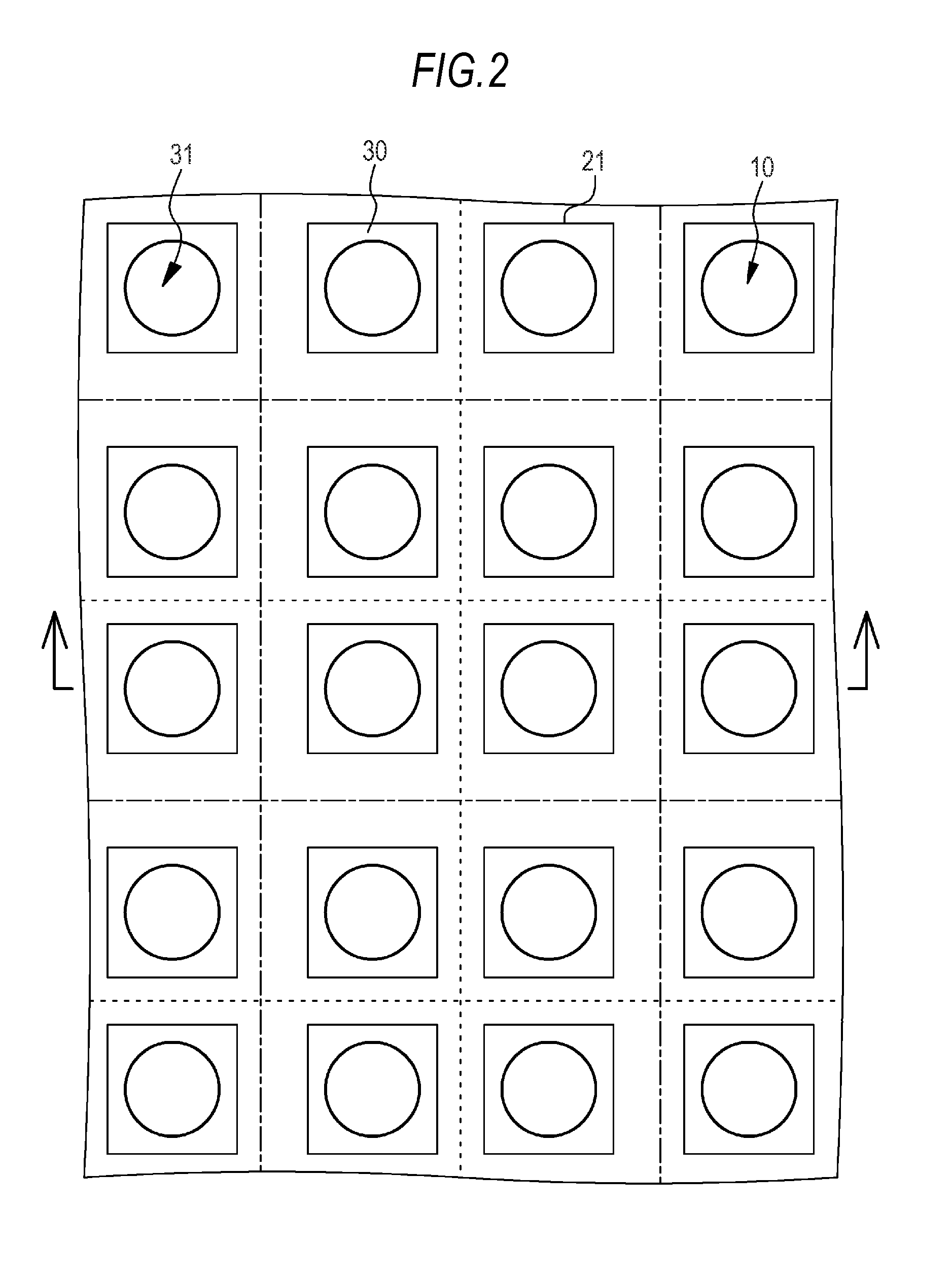
[0076]FIGS. 1A and 1B are schematic partial sectional views of the two-dimensional solid-state imaging device of Example 1 or Examples 2 to 7 described below. FIG. 2 schematically shows arrangement of pixel regions and subpixel regions in the two-dimensional solid-state imaging device of Example 1. FIG. 3A is a schematic partial end view of the pixel regions and the subpixel regions taken along the arrow of FIG. 2. FIG. 3B is a conceptual view regarding arrangement of the pixel regions and the subpixel regions. FIG. 3C is an equivalent circuit diagram of one subpixel region....
example 2
[0091]Example 2 is a modification of Example 1. In Example 1, the center of the opening 31 of each of the four subpixel regions in one pixel region is located at the apex of the virtual square. Meanwhile, in Example 3, the value of M is 3, and the center of the opening 31 of each of the four subpixel regions in one pixel region is located at the apex of a virtual rectangle.
[0092]Specifically, as schematically shown in FIG. 6 regarding the arrangement of the pixel regions and the subpixel regions, the center of the opening 31 of each of the four subpixel regions in one pixel region is located at the apex of the virtual rectangle, and near-field light corresponding to three wavelength components due to surface plasmon polariton resonance excited depending on three wavelength components of the incoming electromagnetic wave and three distances Lm (specifically, m=2, m=3, and m=4) is converted to an electrical signal by the photoelectric conversion elements 21 in the first subpixel regio...
example 3
[0096]Example 3 is also a modification of Example 1. In Example 3, the value of M is 3, and the center of the opening 31 of each of four subpixel regions in one pixel region is located at the apex of the a virtual parallelogram.
[0097]Specifically, as schematically shown in FIG. 7 regarding the arrangement of the pixel regions and the subpixel regions, the center of the opening 31 of each of the four subpixel regions in one pixel region is located at the apex of the virtual parallelogram, and near-field light corresponding to three wavelength components due to surface plasmon polariton resonance excited depending on three wavelength components of the incoming electromagnetic wave and three distances Lm (specifically, m=2, m=3, and m=4) is converted to an electrical signal by the photoelectric conversion elements 21 in the first subpixel region 101 and the m-th subpixel region 10m. This example is the same as Example 2 where the center of the opening 31 of each of the four subpixel re...
PUM
 Abstract
Description
Claims
Application Information