
Photovoltaic cell having nanodots and method for forming the same

a photovoltaic cell and nano-dot technology, applied in the field of photovoltaic cell technology, can solve the problems of economic growth bottleneck and lower the efficiency of the photovoltaic device, and achieve the effect of improving the efficiency of the photovoltaic cell and increasing the mobility of the hol

Inactive Publication Date: 2010-12-02
NAT TAIWAN UNIV
View PDF5 Cites 11 Cited by
  • Summary
  • Abstract
  • Description
  • Claims
  • Application Information

AI Technical Summary

Benefits of technology

[0007]The present invention provides a photovoltaic cell having nanodots and a method for forming the photovoltaic cell, wherein the hole transport material of the photovoltaic cell is mixed with nanodots to form a photovoltaic thin film. The photovoltaic cell using such a photovoltaic thin film exhibits enhanced hole mobility to improve the efficiency of the photovoltaic cell.

Problems solved by technology

As the amounts of conventional resources such as electricity, coal and petroleum are limited, the resource problems have become a bottleneck of economic growth.
Therefore, electrons accumulated in the active layer tend to recombined with the holes to lower the efficiency of the photovoltaic device.

Method used


Image

  • Photovoltaic cell having nanodots and method for forming the same
  • Photovoltaic cell having nanodots and method for forming the same
  • Photovoltaic cell having nanodots and method for forming the same

Examples


Embodiment Construction

[0018]The present invention can be exemplified but not limited by various embodiments as described hereinafter.

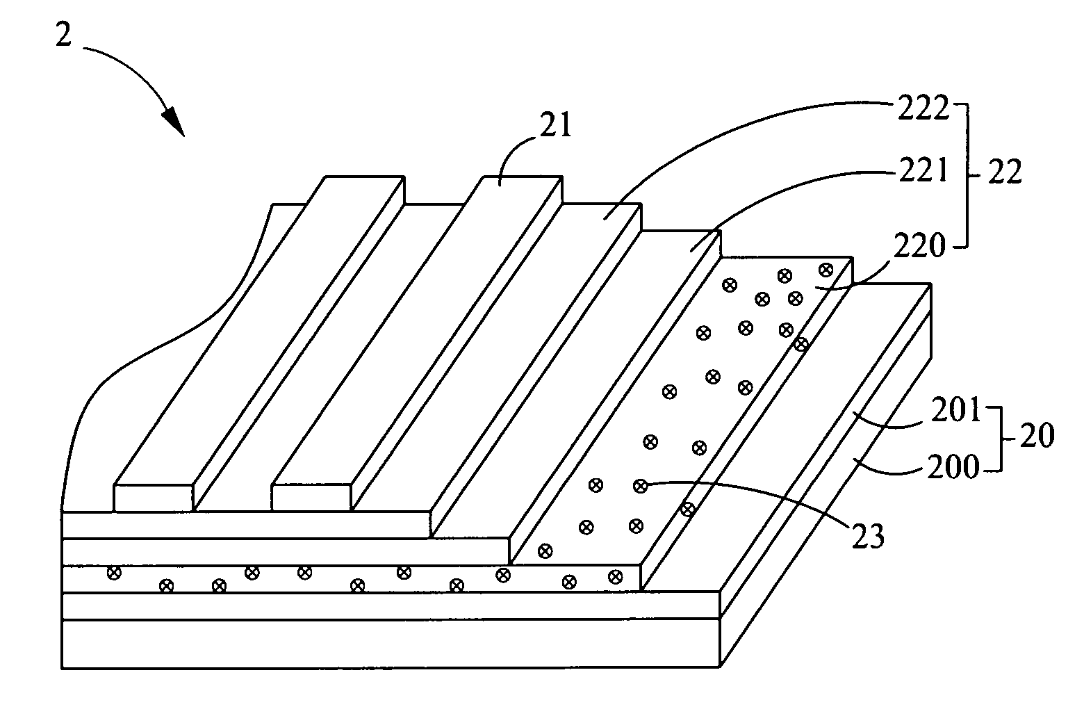
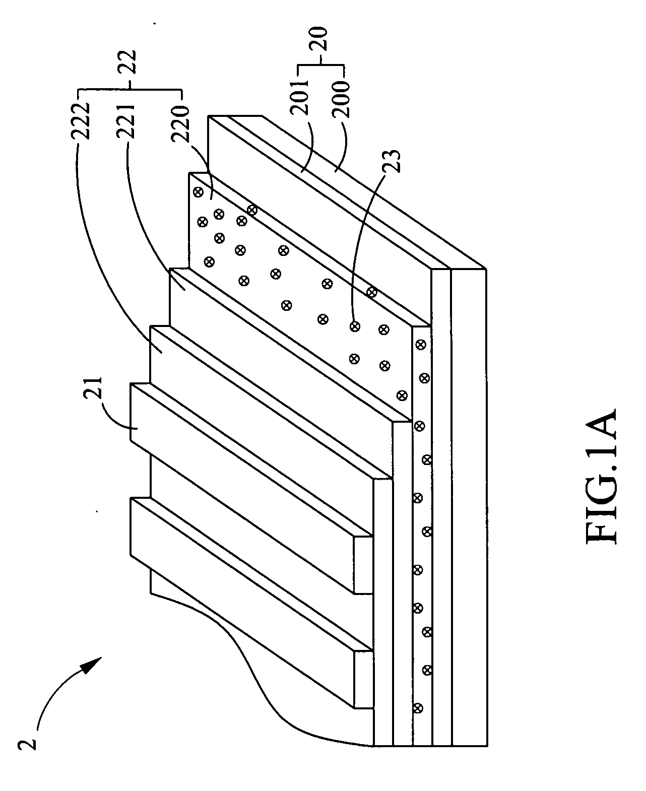
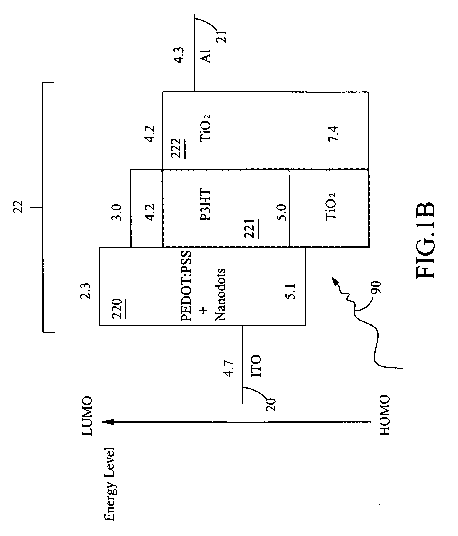
[0019]Please refer to FIG. 1A, which schematically depicts a photovoltaic cell according to the present invention. In the present embodiment, the photovoltaic cell 2 comprises a first electrode 20, a second electrode 21 and a photovoltaic conversion layer 22 disposed between the first and second electrodes 20 and 21 so as to convert incident light into a plurality of hole-electron pairs. In the present embodiment, the first electrode 20 is a transparent electrode comprising a substrate 200 and a conductive layer 201 formed on the substrate 200. The substrate 200 may be a transparent substrate, such as a glass substrate or a plastic substrate. The conductive layer 201 may comprise a transparent conductive material such as indium-tin oxide (ITO), aluminum-zinc oxide (AZO) or zinc oxide (ZnO), but is not limited thereto. In the present embodiment, the conductive layer 200 comp...


PUM

PropertyMeasurementUnit
Electrical conductoraaaaaaaaaa
Transparencyaaaaaaaaaa
Transport propertiesaaaaaaaaaa

Abstract

The present invention provides a photovoltaic cell comprising a photovoltaic conversion layer and a pair of electrodes. The photovoltaic conversion layer, being capable of converting incident light into a plurality hole-electron pairs, comprises a hole transport layer including a plurality of nanodots mixed therein for transporting the holes generated from the photovoltaic effect. The pair of electrodes are coupled respectively to two sides of the photovoltaic conversion layer for conducting holes and electrons. In another embodiment, the present invention further provides a method for forming the photovoltaic cell, wherein the nanodots are mixed in a solution formed of a hole transport material and then a hole transport layer having the nanodots is formed on a conductive substrate. In the photovoltaic cell having nanodots of the present invention, the hole mobility is enhanced so as to improve the efficiency of the photovoltaic cell.

Description

FIELD OF THE PRESENT INVENTION [0001]The present invention generally relates to a photovoltaic cell technology and, more particularly, to a photovoltaic cell having nanodots with increased hole transport efficiency and a method for forming the photovoltaic cell.BACKGROUND OF THE PRESENT INVENTION [0002]As the amounts of conventional resources such as electricity, coal and petroleum are limited, the resource problems have become a bottleneck of economic growth. More and more countries have launched researches on solar energy as a potential motive force for economic development. The solar energy, as a renewable energy resource, has attracted tremendous amount of attention. The solar energy is realized using photovoltaic cells with less power consumption and environment friendliness. In recent years, with the increasing demand in the solar energy, the manufacturing technology of photovoltaic cells has advanced significantly. Therefore, the solar energy has been the fastest developing i...

Claims


Application Information

Patent Timeline
IPC IPC(8): H01L31/00H01L51/46
CPCH01L51/0036H01L51/0037Y02E10/549H01L51/426H01L51/4226Y02P70/50H10K85/1135H10K85/113H10K30/151H10K30/50H10K30/352H10K30/35
Inventor SU, WEI-FANGJOU, JWO-HUEIWANG, WEI-BENLIN, JHIH-FONG
Owner NAT TAIWAN UNIV
Learn More