Electronic Device Having an Electrode With Enhanced Injection Properties

an electronic device and enhanced injection technology, applied in thermoelectric devices, coatings, transportation and packaging, etc., can solve the problems of reducing the lifetime of the known organic light-emitting diode, and reducing the operating voltage. , to achieve the effect of enhancing the injection property, reducing the operating voltage, and increasing the light-emitting efficiency

Active Publication Date: 2010-12-09
IBM CORP
View PDF7 Cites 0 Cited by
  • Summary
  • Abstract
  • Description
  • Claims
  • Application Information

AI Technical Summary

Benefits of technology

[0010]It is therefore an aspect of the present invention to provide methods for producing an electronic device, especially an organic light-emitting diode, having an electrode with enhanced injection properties, so that a lower operating voltage, a higher light emission efficiency, and a longer lifetime can be achieved.
[0011]It is a further aspect of the present invention to provide an electronic device, especially an organic light-emitting diode, having an electrode with enhanced injection properties, so that a lower operating voltage, a higher light emission efficiency, and a longer lifetime can be achieved.
[0014]Then, the molecular charge transfer material is cross-linked in order to enhance the injection property of the first electrode. The cross-linking step may for example be performed by irradiating the molecular charge transfer material with an electron beam, so that a polymerization and cross-linking of the molecular charge transfer material takes place. The molecular charge transfer material does not need to be cross-linked as a whole, it is in fact sufficient to cross-link only a part of the material. However, it is most advantageous to cross-link the whole molecular charge transfer material. The cross-linking provides a higher thermal stability of the layer of molecular charge transfer material.

Problems solved by technology

This originates inter-alia from the fact that the injection of charge carriers, i.e. electrons or holes, from the electrodes into the organic layer is less efficient, i.e. the common organic light-emitting diodes do not have electrodes which exhibit ohmic or barrier-less injection.
Though the above-described arrangement is able to enhance the injection properties and to reduce the operating voltage, the enhancement of the injection properties and the reduction of the operating voltage are still not sufficient.
Further, the lifetime of the known organic light-emitting diode is decreased, i.e. the diode is subjected to an accelerated ageing, which leads to a decrease of the luminosity of the emitter material (EM).
Thus, already after a short running time the light emission efficiency is low.

Method used


Image

  • Electronic Device Having an Electrode With Enhanced Injection Properties
  • Electronic Device Having an Electrode With Enhanced Injection Properties
  • Electronic Device Having an Electrode With Enhanced Injection Properties

Examples


Embodiment Construction

[0027]The present invention provides methods for producing an electronic device, especially an organic light-emitting diode, having an electrode with enhanced injection properties, so that a lower operating voltage, a higher light emission efficiency, and a longer lifetime can be achieved. The present invention also provides an electronic device, especially an organic light-emitting diode, having an electrode with enhanced injection properties, so that a lower operating voltage, a higher light emission efficiency, and a longer lifetime can be achieved.

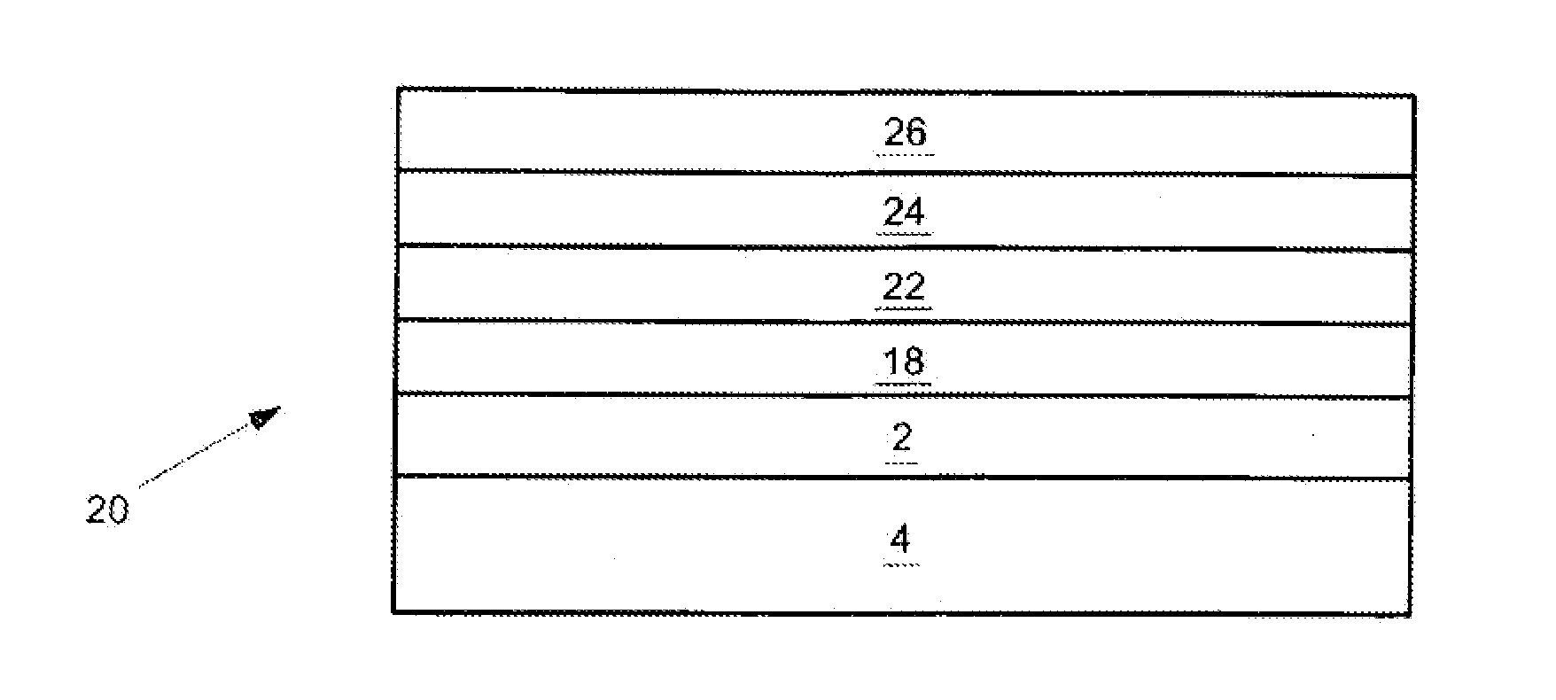
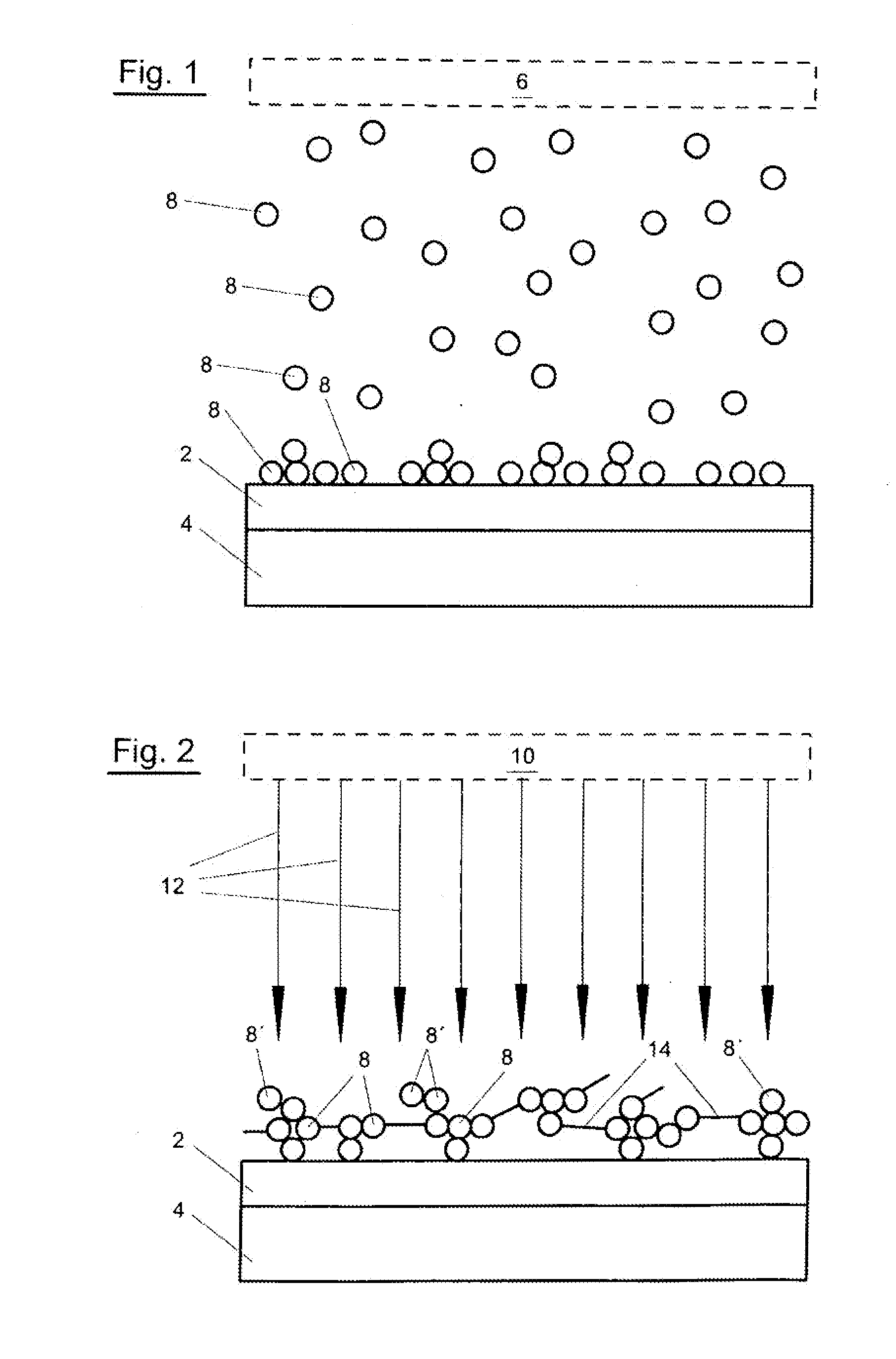
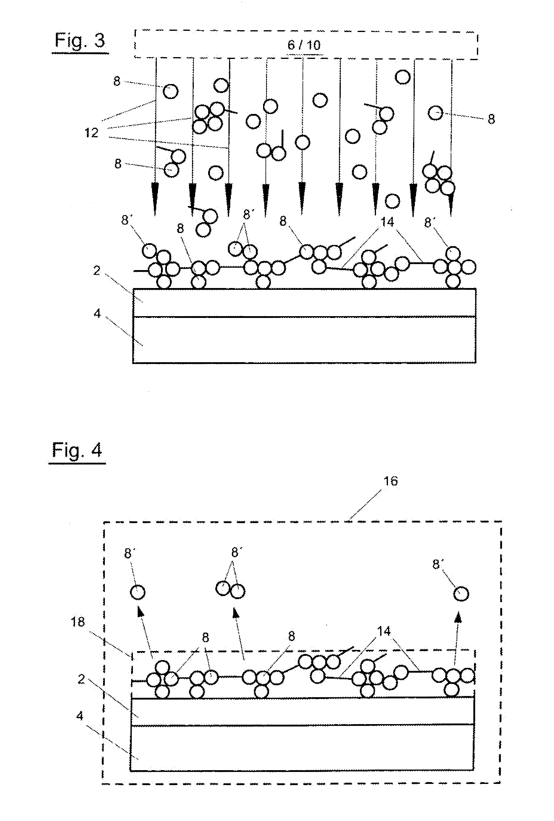
[0028]In an example embodiment, a method for producing an electronic device having an electrode with enhanced injection properties according to the invention includes the following steps. First, a first electrode is provided. The first electrode may for example later be used as a cathode or an anode in the final electronic device. The first electrode, which will be used as an anode, may for example comprise an Indium-Tin-Oxide (ITO) la...


PUM


Abstract

An electronic device having an electrode with enhanced injection properties comprising a first electrode and a first layer of cross-linked molecular charge transfer material on the first electrode. The cross-linked molecular charge transfer material may be an acceptor, which may consist of at least one of: TNF, TN9(CN)2F, TeNF, TeCIBQ, TCNB, DCNQ, and TCAQ. The cross-linked molecular charge transfer material may also be a donor, which may consist of at least one of: Terpy, Ru(terpy)2 TTN, and crystal violet.

Description

CROSS-REFERENCE TO RELATED APPLICATIONS[0001]This application is a divisional of U.S. patent application Ser. No. 11 / 205,232, filed Oct. 19, 2006, entitled “Electronic device having an electrode with enhanced injection properties”, the contents of which are incorporated by reference herein in their entirety.BACKGROUND OF THE INVENTION[0002]The present invention relates to producing an electronic device, such as an organic light-emitting diode (OLED), having an electrode with enhanced injection properties. Further, the present invention relates to an electronic device comprising an electrode with enhanced injection properties.[0003]Organic light emitting diodes (OLEDs) represent a promising technology for display applications or illumination applications. A typical light-emitting diode includes a substrate. On the substrate there is arranged a first electrode, which usually acts as a hole-injecting anode. On the anode there is provided a luminescent region comprising an organic elect...

Claims


Application Information

Patent Timeline
Patent Type & Authority Applications(United States)
IPC IPC(8): H01L51/54H01L51/56
CPCH01L51/0003H01L51/0051H01L51/0062H01L51/56H01L51/5088H01L51/5092H01L51/0086Y10T428/31504H10K71/12H10K85/611H10K85/649H10K85/344H10K50/171H10K50/17H10K71/00
Inventor BRUNSCHWILER, THOMASKARG, SIEGFRIED F.RIESS, WALTER
Owner IBM CORP
Why Eureka
Try Eureka