Power factor correction circuit

a power factor and circuit technology, applied in the emergency protective circuit arrangement, emergency protection circuit arrangement, energy industry, etc., can solve the problems of complex circuit configuration, and inability to achieve overcurrent bypass, etc., to achieve the effect of reducing the changing rate of current flowing through the inductor, reducing the power loss caused in the diode in the second rectifying bridge circuit, and reducing the power loss caused in the switching device and the rectifying devi

Inactive Publication Date: 2010-12-09
FUJI ELECTRIC CO LTD
View PDF4 Cites 15 Cited by
  • Summary
  • Abstract
  • Description
  • Claims
  • Application Information

AI Technical Summary

Benefits of technology

[0035](1) The power loss caused in the diode in the second rectifying bridge circuit is reduced and the overcurrent caused at the start of operation of the circuit or at a power fail recovery is made not to flow through the diodes in the first rectifying bridge circuit (the high-speed diodes), nor through the parasitic diodes of the switching devices (the MOSFETs).
[0036](2) The changing rate of the current flowing through the inductor is reduced and the power losses caused in the switching devices and the rectifying devices are reduced.
[0037](3) The power losses caused in the inductors, switching devices and rectifying devices are dispersed. The downsizing of a heat sink for cooling the semiconductor devices and the downsizing of inductors and such component parts are facilitated.

Problems solved by technology

Therefore, the circuit configuration is complicated and the manufacturing costs of the circuit soar.
If the power fail time is shorter than the time necessary for detecting the power fail, it will be impossible to accomplish the overcurrent bypass, since the power fail is not detected.

Method used


Image

  • Power factor correction circuit
  • Power factor correction circuit
  • Power factor correction circuit

Examples


first embodiment

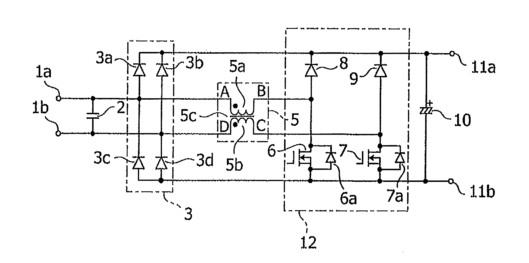
[0062]FIG. 1 is a circuit diagram showing a power factor correction circuit according to the invention. In FIG. 1, the same reference numerals as used in FIG. 18 are used to designate the same constituent elements and their duplicated description are omitted for the sake of simplicity.

[0063]The power factor correction circuit according to the first embodiment is different from the conventional power factor correction circuit shown in FIG. 18 in that rectifying bridge circuit 3 is interposed between AC input terminals 1a and 1b and rectifying bridge circuit 12. The power factor correction circuit shown in FIG. 1 is different from the conventional power factor correction circuit shown in FIG. 18 also in that inductor 4a is interposed between AC input terminal 1a and the first input of rectifying bridge circuit 12, and inductor 4b is interposed between AC input terminal 1b and the second input of rectifying bridge circuit 12. In contrast, in the conventional power factor correction cir...

second embodiment

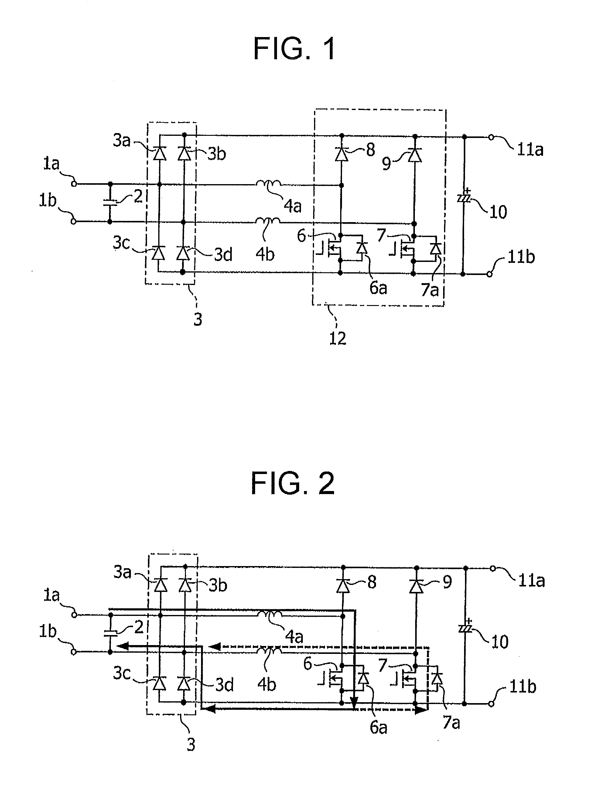
[0072]FIG. 5 is a circuit diagram showing a power factor correction circuit according to the invention.

[0073]The power factor correction circuit according to the second embodiment is different from the power factor correction circuit according to the first embodiment in that inductors 4a and 4b are replaced by inductor 5 in FIG. 5.

[0074]FIG. 6 is a drawing showing the detailed structure of inductor 5 shown in FIG. 5.

[0075]As shown in FIG. 6, inductor 5 includes windings 5a and 5b wound around core 5c to be coupled magnetically to each other. Windings 5a and 5b are wound such that the direction of the magnetic flux ψ1 generated by the current I1 that flows from terminal A to terminal B is opposite to the direction of the magnetic flux ψ2 generated by the current I2 that flows from terminal C to terminal D.

[0076]Next, the operations of the power factor correction circuit according to the second embodiment will be described below.

[0077]First, steady-state operations will be described. ...

third embodiment

[0098]The power factor correction circuit facilitates reducing the electric power transmitted through one group of the circuit as compared with the circuit shown in FIG. 5. Therefore, the losses caused by inductors 5, 5′, MOSFETs 6, 6′, 7, 7′, and diodes 8, 8′, 9, 9′ are dispersed, and, as a result, the downsizing of the heat sink for cooling the semiconductor devices (MOSFETs 6, 6′, 7, 7′, etc.) and the downsizing of inductors 5 and 5′ are facilitated.

[0099]The circuit, a plurality of which is connected in parallel, is not always limited to the circuit shown in FIG. 5. The circuit, a plurality of which is to be connected in parallel, may be the circuit shown in FIG. 1 with no problem. The number of groups connected in parallel is not always limited to 2. Three or more groups of the circuit may be connected in parallel with no problem. In the power factor correction circuit shown in FIG. 13, rectifying bridge circuit 3 and smoothing capacitor 10 are used commonly for the circuit gr...


PUM


Abstract

A power factor correction circuit includes a filter capacitor interposed between AC input terminals, a first inductor interposed between the first end of the filter capacitor and an input of a first rectifying bridge circuit, and a second inductor interposed between the second end of the filter capacitor and another input of the first rectifying bridge circuit. The power factor correction circuit further includes a second rectifying bridge circuit including inputs connected to AC input terminals, and outputs connected to a smoothing capacitor. A control circuit controls switching devices in the first rectifying bridge circuit. The power factor correction circuit can facilitate preventing an overcurrent from flowing through diodes and parasitic diodes in the switching devices, using a simple configuration.

Description

CROSS-REFERENCE TO RELATED APPLICATIONS[0001]This application claims priority under 35 U.S.C. §119 from JP PA 2009-133886, filed Jun. 3, 2009, the entirety of which is incorporated herein by reference.FIELD OF THE INVENTION[0002]The present invention relates to a power factor correction circuit that controls the current flowing through AC input terminals by the ON-OFF operation of a switching device to be sinusoidal for obtaining a DC output.BACKGROUND[0003]FIG. 17 is a circuit diagram of a conventional power factor correction circuit. Referring now to FIG. 17, the conventional power factor correction circuit conducts the full-wave-rectification of an AC voltage fed to AC input terminals 1a and 1b with rectifying bridge circuit 3 formed of diodes 3a through 3d. The conventional power factor correction circuit boosts the output voltage fed from rectifying bridge circuit 3 with a boost chopper circuit formed of inductor 4, MOSFET 6 working as a switching device, diode 8, and smoothing...

Claims


Application Information

Patent Timeline
Patent Type & Authority Applications(United States)
IPC IPC(8): H02M7/06
CPCY02B70/126H02M1/4225Y02B70/10Y02P80/10H02M1/0085
Inventor NISHIKAWA, YUKIHIRO
Owner FUJI ELECTRIC CO LTD
Why Eureka
Try Eureka