Device for detection and/or emission of electromagnetic radiation and method for fabricating such a device
- Summary
- Abstract
- Description
- Claims
- Application Information
AI Technical Summary
Benefits of technology
Problems solved by technology
Method used
Image

Examples
first embodiment
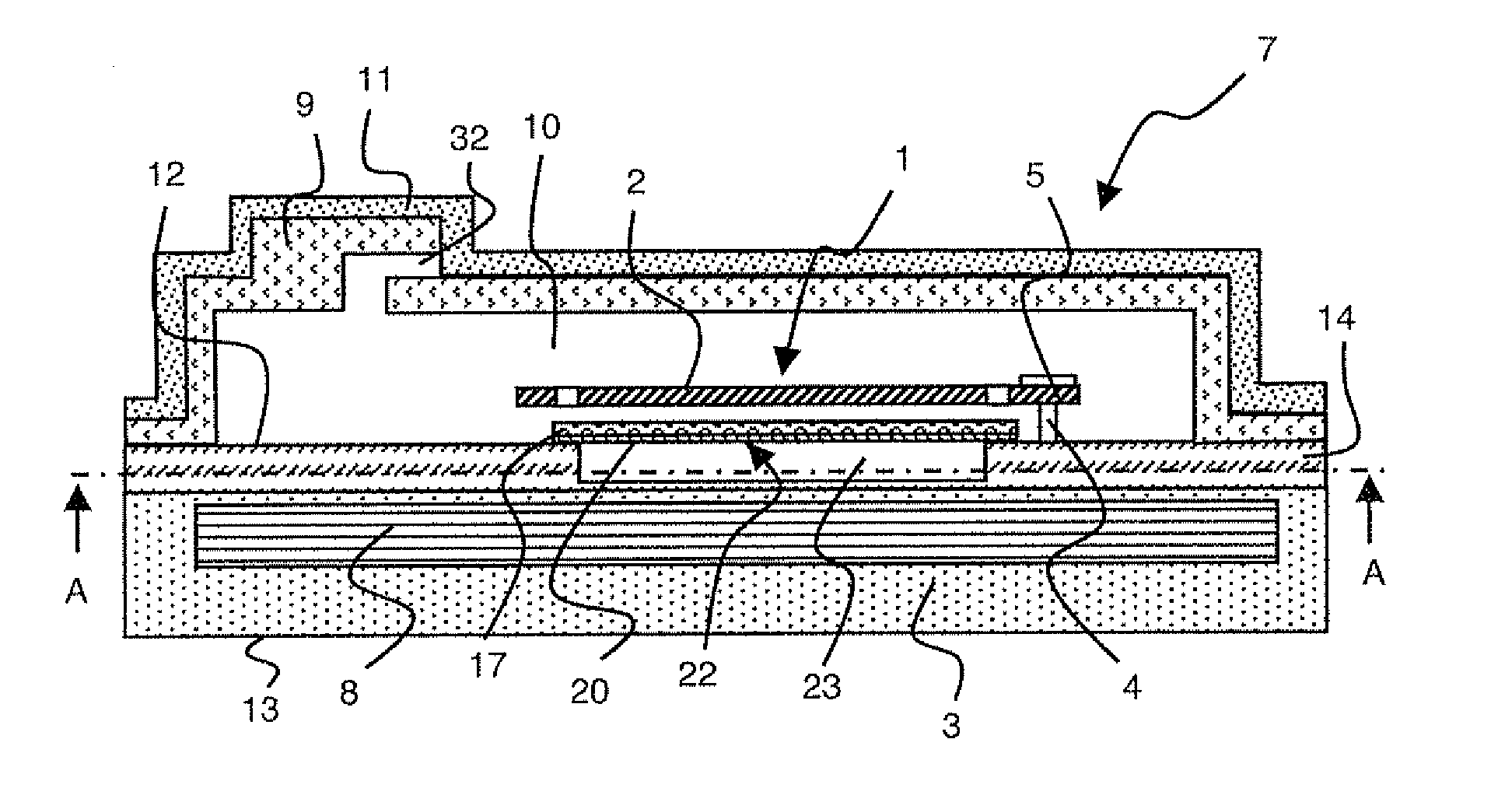
[0064]A method for fabricating the device for detection and / or emission of electromagnetic radiation represented in FIG. 6 comprises formation of free space 23 between reflector / getter assembly 22 and front surface 12 of substrate 3. Free space 23 is produced by an etching step (FIG. 8) of superficial passivation layer 14 constituting front surface 12 of substrate 3. This formation step of free space 23 is integrated in a conventional encapsulation device fabrication method well known to the person skilled in the art and comprising usual microelectronics techniques, in particular the range of micromachining techniques such as deposition and etching of thin layers.
[0065]The different characteristic steps involved in fabrication of the device according to FIG. 6 are represented in FIGS. 8 to 12. As represented in FIG. 8, we start out with a substrate 3 formed by a silicon wafer, for example with a thickness of 500 μm and a thin layer of SiO with a thickness comprised between 1 μm and...
third embodiment
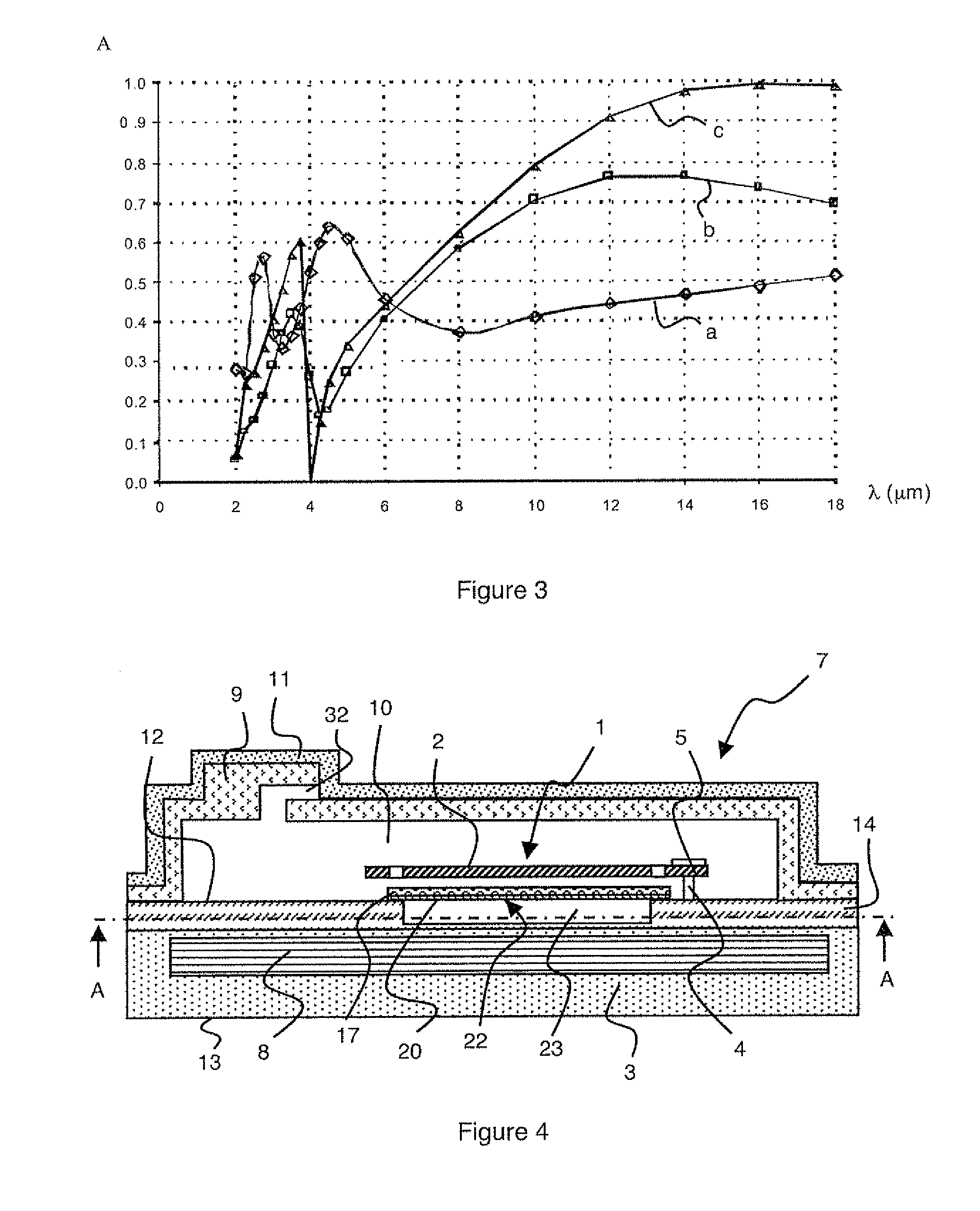
[0091] represented in FIG. 18, reflector / getter assembly 22 is formed by two first getters 20 and 29 and reflector 17. Getters 20 and 29 are arranged in such a way that each of them has an accessible surface 24 released by free space 23. This embodiment enables the efficiency of pumping to be optimized by combining the specificities of the different getter materials. Getter 20 can for example be made from a material selectively absorbing hydrogen and getter 29 from a material selectively absorbing oxygen.
[0092]The method for fabricating such a device comprises a deposition step of reflector / getter assembly 22 according to the successive steps described in the following.
[0093]As represented in FIG. 19, getter 20 is deposited and etched if required on front surface 12 of substrate 3, between anchoring areas 33 and at a distance from these anchoring areas 33.
[0094]A first barrier layer 26 and a second barrier layer 27 are advantageously deposited and etched if required so as to be situ...
PUM
 Abstract
Description
Claims
Application Information