Solid-state imaging device, imaging system, and method of driving solid-state imaging device

a solid-state imaging and imaging device technology, applied in the field of solid-state imaging devices, imaging systems, and driving solid-state imaging devices, can solve the problems of increasing power consumption, processing becomes complicated, and the chip size increases, so as to suppress the degradation of the sn ratio of good images, suppress the increase of the chip size of the imaging device, and suppress the increase of the power consumption of the sensor

Inactive Publication Date: 2010-12-23
CANON KK
View PDF16 Cites 39 Cited by
  • Summary
  • Abstract
  • Description
  • Claims
  • Application Information

AI Technical Summary

Benefits of technology

[0009]It is an object of the present invention to provide a solid-state imaging device, an imaging system, and a method of driving a solid-state imaging device, all capable of obtaining a good image suppressing the degradation of the SN ratio there...

Problems solved by technology

If the gain of each pixel is severally adjusted like the technique disclosed in the Japanese Patent Application Laid-Open No. 2004-015701 in such a case, then the processing becomes complicated and power consumption also increases.
Moreover, if the circuits performing signal processing ar...

Method used


Image

  • Solid-state imaging device, imaging system, and method of driving solid-state imaging device
  • Solid-state imaging device, imaging system, and method of driving solid-state imaging device
  • Solid-state imaging device, imaging system, and method of driving solid-state imaging device

Examples


first exemplary embodiment

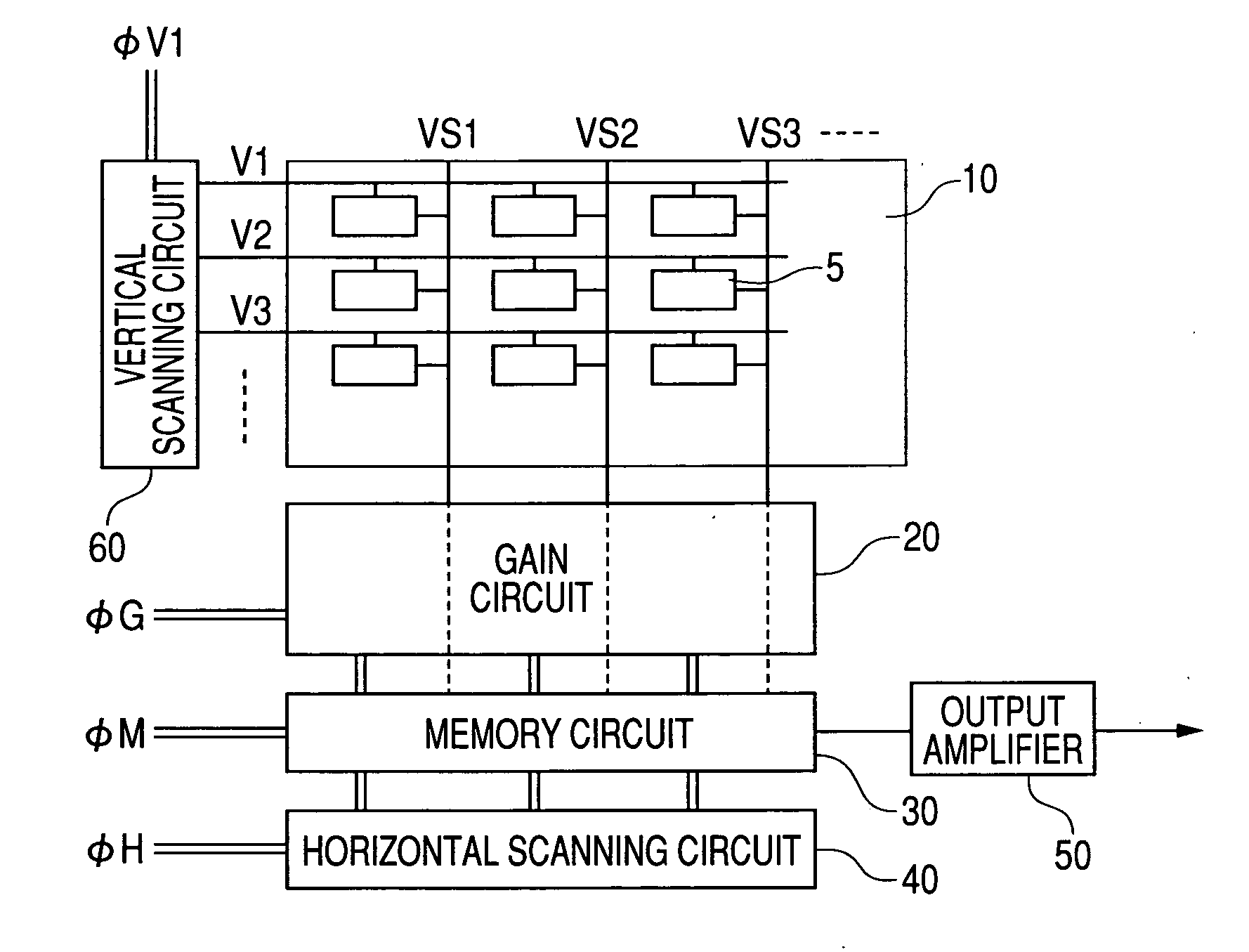
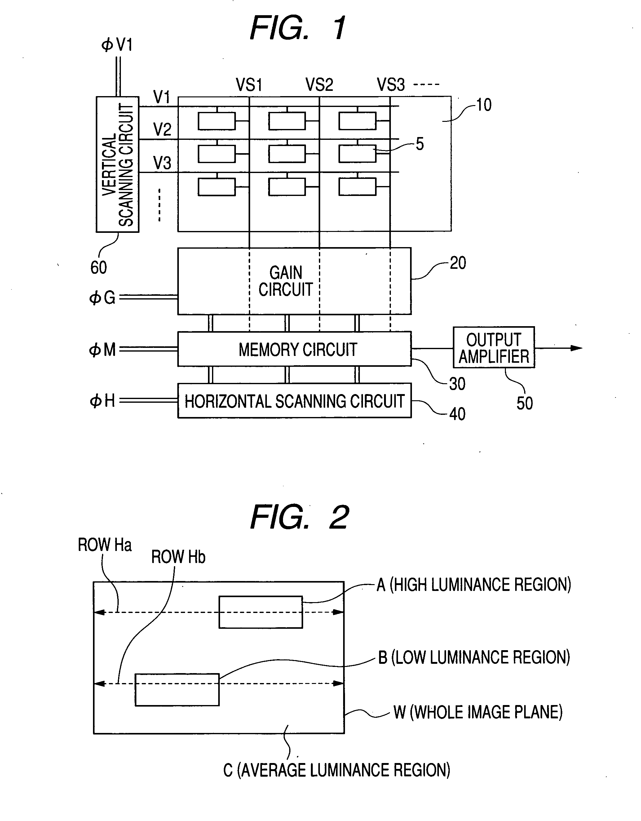
[0028]A first exemplary embodiment according to the present invention is described with reference to FIGS. 1 to 4. FIG. 1 is a schematic view illustrating an example of a solid-state imaging device according to the first exemplary embodiment of the present invention. Each configuration in the figure is formed on the same semiconductor substrate.

[0029]Pixels 5 are arranged in a matrix in a pixel portion 10 of the solid-state imaging device 100. The pixels 5 in the same row are connected by each of the control lines V1, V2, . . . , Vn in common, and the signals of the pixels 5 in the same row are read to vertical signal lines VS1, VS2, . . . , VSn at the same timing when the pixels 5 receive a signal from a vertical scanning circuit 60. The signals read on the vertical signal lines VS1, VS2, . . . , VSn are input into a gain circuit 20, which is a variable gain unit including variable gain amplifiers provided on each of the vertical signal lines VS1, VS2, . . . , VSn. The gains of the...

second exemplary embodiment

[0044]A second exemplary embodiment according to the present invention is described with reference to FIGS. 7 and 8. In the first exemplary embodiment, the example of reading all regions A, B, and C in the imaging plane during one frame period has been described. On the other hand, in the present exemplary embodiment, an exemplary embodiment of reading partial regions A and B in different frames from the frame in which the whole region W is read by thinning out the read of the whole region W is described.

[0045]FIG. 7 is a diagram illustrating a situation of an imaging plane and the timing of scanning each row in the imaging plane. In FIG. 7, pixel rows Va1, Va2, . . . , Va6, illustrated by being hatched by meshes, are read in a frame F1. Pixel rows Vb1, . . . , Vb5, which are included in the partial region A and are not the pixel rows Van (n: natural numbers), are read in a frame F2. Pixel rows Vb6, . . . , Vb10, which are included in the partial region B and are not the pixel rows ...

third exemplary embodiment

[0054]A third exemplary embodiment according to the present invention is described with reference to FIGS. 7 and 9-13. In the present exemplary embodiment, the case of performing not only the control of the gains of the amplifiers in the imaging plane as illustrated in FIG. 7 but also the control of charge accumulating time is discussed. The frames F1, F2, and F3 are repeated also in the present exemplary embodiment similarly to the second exemplary embodiment.

[0055]FIG. 9 is a schematic view illustrating an example of a solid-state imaging device according to the present exemplary embodiment, and the same components as those illustrated in FIG. 1 are denoted by the same reference numerals as those in FIG. 1. The solid-state imaging device of the present exemplary embodiment is different from that illustrated in FIG. 1 in being provided with a vertical scanning circuit 61 (VSR-B), which is a charge accumulation control unit controlled by a signal φV2, in addition to the vertical sca...


PUM


Abstract

The invention provides a solid state imaging device and imaging system, both capable of obtaining a good image suppressing the reduction of the SN ratio thereof, suppressing the increase of the chip size of the imaging device and suppressing the increase of power consumption of a sensor without performing complicated processing even if there are regions different in luminance mutually in an imaging plane. Variable gain units provided correspondingly to columns of pixels amplify the signals from the pixels by different gains group by group of the pixels each group including a plurality of pixels according to the signals from the outside.

Description

TECHNICAL FILED[0001]The present invention relates to solid-state imaging device and an imaging system using the solid-state imaging device, and more particularly to a solid-state imaging device controlling the brightness of an image in a imaging plane.BACKGROUND ART[0002]When an object is imaged, there may be a light region and a dark region in an imaging plane according to the condition of a light source to the object. As a technique of performing the exposure control of an imaging device under such an imaging condition, the techniques disclosed in Japanese Patent Application Laid-Open No. 2004-15701 and Japanese Patent Application Laid-Open No. 2001-145005 exist.[0003]The solid-state imaging device disclosed in the Japanese Patent Application Laid-Open No. 2004-15701 provides the function of detecting the magnitude of each pixel signal individually to set a gain to the magnitude of the signal individually to the column region portion of a sensor.[0004]Moreover, the Japanese Paten...

Claims


Application Information

Patent Timeline
IPC IPC(8): H04N9/68H04N5/335H04N5/353H04N5/357H04N5/376H04N5/378
CPCH04N5/2351H04N5/2355H04N5/378H04N5/355H04N5/37457H04N5/243H04N23/741H04N23/71H04N23/76H04N25/57H04N25/778H04N25/75
Inventor HASHIMOTO, SEIJIOTA, KEISUKESHIGETA, KAZUYUKIOHYA, TAKERU
Owner CANON KK
Why Eureka
Try Eureka