Plasma processing apparatus and plasma processing method

Inactive Publication Date: 2010-12-30
HITACHI HIGH-TECH CORP
View PDF4 Cites 96 Cited by
  • Summary
  • Abstract
  • Description
  • Claims
  • Application Information

AI Technical Summary

Benefits of technology

[0025]Still further, in the above plasma processing apparatus, the control means controls the temperature of a coolant to be allowed to flow in a lower portion of the focus ring according to the electric power allocated to the focus ring.
[0026]Still further, in the above plasma processing apparatus, the control means controls the pressure of the heat transfer gas and the temperature of a coolant to be allowed to flow in the lower portion of the focus ring according to the electric power allocated to the focus ring.
[0027]Still further, according to the present invention, there is provided a plasma processing method for processing, through the effect of plasma, a substrate to be processed placed on a substrate stage by supplying a gas to a vacuum vessel, wherein a high frequency bias power supply applies, to the substrate stage, a predetermined high frequency bias electric power being different from a high frequency electric power supply for generating plasma; wherein electric power allocation means allocates and applies a high frequency bias electric power outputted from the high frequency bias power supply to a focus ring disposed in the periphery of the substrate to be processed; wherein, according to an

Problems solved by technology

However, another problem as follows arises.
In this way, when the temperature of the wafer edge portion rises, there occur fatal problems to the etching characteristics such as an occurrence of etching stop in the wafer edge portion, an o

Method used


Image

  • Plasma processing apparatus and plasma processing method
  • Plasma processing apparatus and plasma processing method
  • Plasma processing apparatus and plasma processing method

Examples


Embodiment Construction

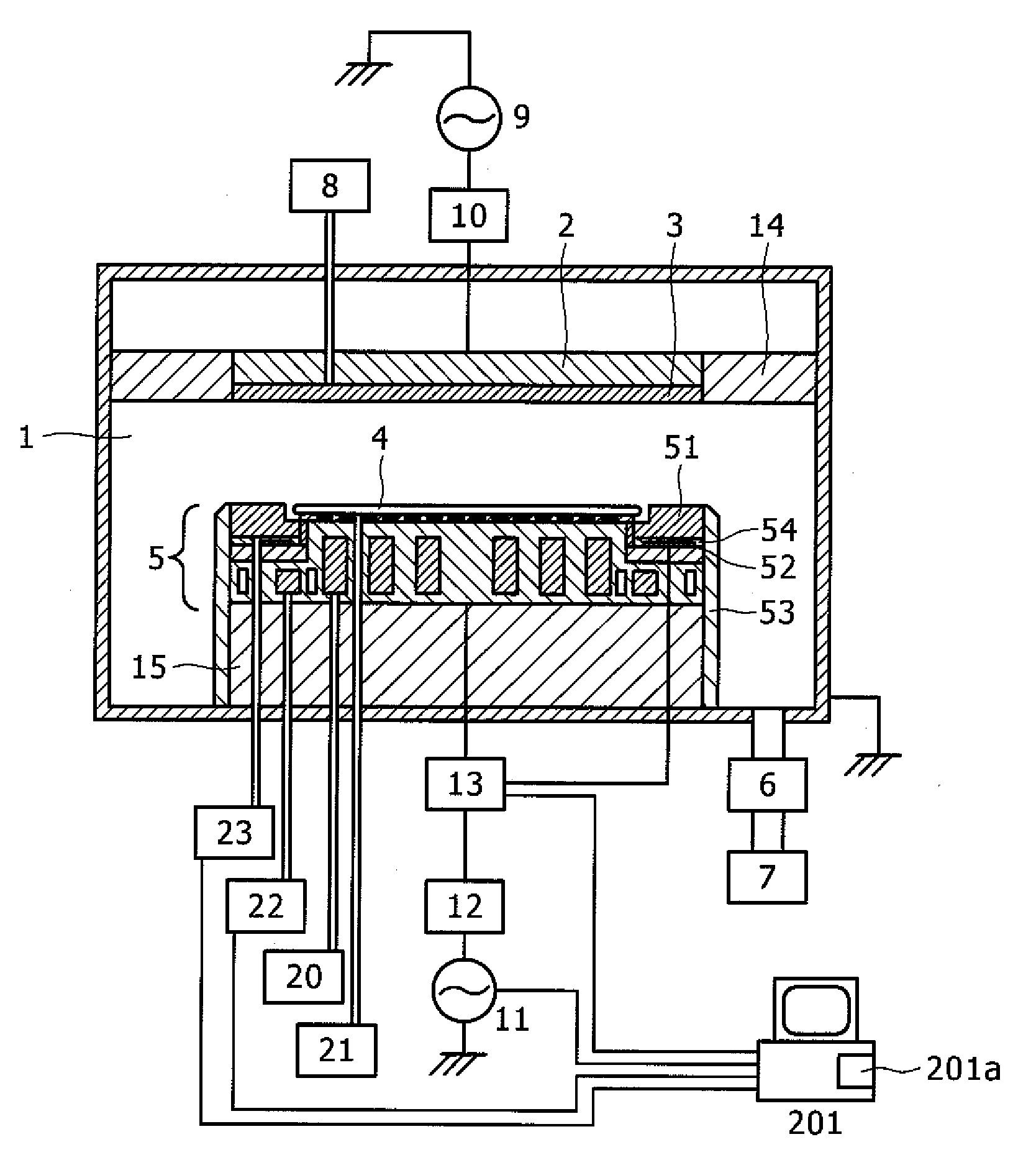
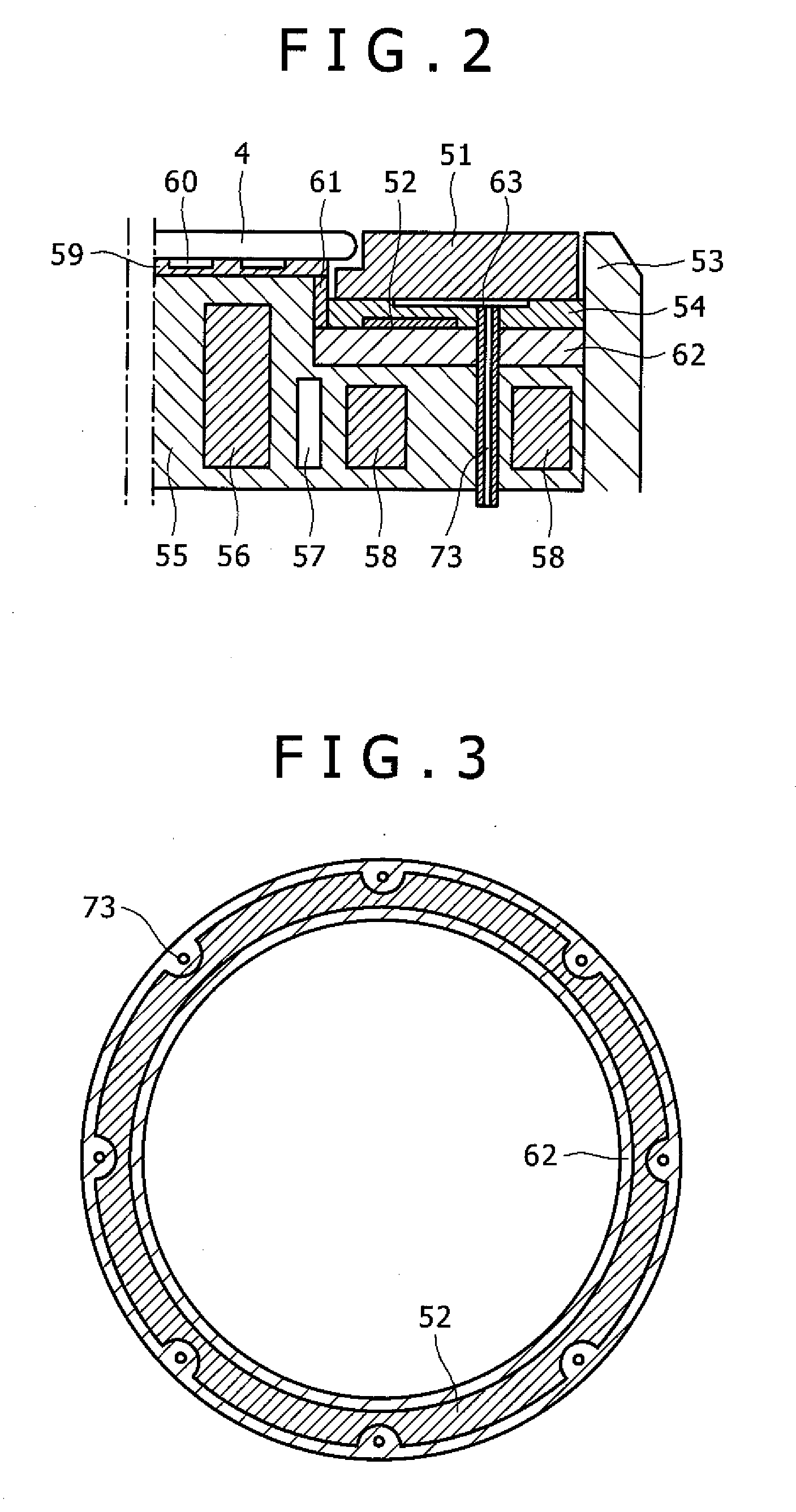
[0042]Now, with reference to FIGS. 1 to 7, a first embodiment of the present invention will be described. FIG. 1 is a longitudinal cross section of a plasma processing apparatus according to the present embodiment, FIG. 2 is a longitudinal cross section of the outer periphery of the substrate stage according to the present embodiment, FIG. 3 is a plan view showing one example of an electrode pattern and a pattern of a heat transfer gas hole provided below the focus ring, and FIG. 4 is a longitudinal cross section showing a feeding part to an electrode layer provided below the focus ring.

[0043]In FIG. 1, according to the plasma processing apparatus of the present embodiment, there are provided, in a vacuum vessel 1, an upper electrode 2, a shower plate 3, an insulating members 14 and 15, and a substrate stage 5 for loading a disc-like wafer to be processed (substrate to be processed) 4. On the substrate stage, there is provided an almost circular ring-shaped member (focus ring) 51 in...


PUM

PropertyMeasurementUnit
Temperatureaaaaaaaaaa
Timeaaaaaaaaaa
Pressureaaaaaaaaaa

Abstract

An electrostatic adsorption layer, an electrode layer, and an insulating layer are provided in a lower portion of a focus ring disposed in an outer periphery of a substrate stage. A high frequency bias is applied to the focus ring by applying a high frequency electric power to the electrode layer. Further, the focus ring is electrostatically chucked to the electrostatic chucking layer and a heat transfer gas is provided between the focus ring and the electrostatic adsorption layer. Thus, the focus ring can be cooled and the temperature of the focus ring is controlled to a predetermined value. With this structure, an etching characteristic at a wafer edge portion can be maintained favorably for a long time. Also, a yield rate at the edge portion can be favorably maintained for a long time, a wet period can be prolonged, and the device operation rate can be improved.

Description

BACKGROUND OF THE INVENTION[0001]1. Field of the Invention[0002]The present invention relates to a dry etching apparatus (plasma processing apparatus) and an etching method for etching an insulating film. For example, it relates to a plasma processing apparatus and a plasma processing method which can, in particular, suppress degradation of etching characteristics such as slanting (tilting) of a hole taking place at a wafer edge, mask clogging, and reduction of etching selectivity when a pattern of a sample to be processed is a high aspect-ratio contact hole.[0003]2. Description of the Related Art[0004]With respect to a memory device represented by DRAM (Dynamic Random Access Memory), as integration progresses, it becomes important to maintain capacity of a capacitor. When roughly classifying capacitor structures, there are a trench capacitor in which a deep trench is formed in a silicon substrate, and a stack capacitor in which a capacitor is formed in an upper portion of a transis...

Claims


Application Information

Patent Timeline
IPC IPC(8): B44C1/22C23F1/08
CPCH01J37/20H01J37/32623H01L21/68735H01J2237/2001H01L21/6831H01J37/32642H01L21/3065H01L21/205
Inventor MAEDA, KENJIYOKOGAWA, KENETSUTAMURA, TOMOYUKIHIROZANE, KAZUYUKIICHINO, TAKAMASA
Owner HITACHI HIGH-TECH CORP
Why Eureka
Try Eureka