Optical filter, solid-state imaging element having the filter, and imaging apparatus

a solid-state imaging element and filter technology, applied in the field of optical filters, can solve the problems of not achieving the color filter for blue, which constitutes the three primary colors, and achieve the effect of reducing the dependence on the polarization of incident light and high transmittance in the wavelength region

Inactive Publication Date: 2010-12-30
CANON KK
View PDF6 Cites 32 Cited by
  • Summary
  • Abstract
  • Description
  • Claims
  • Application Information

AI Technical Summary

Benefits of technology

[0012]The present invention can provide an optical filter that has a minimized dependency on the polarization of incident light and has high transmittance in the wavelength region of blue light.

Problems solved by technology

Such strong polarization dependency causes inconvenience, for example, when the filter is used in an image sensor of a digital camera or the like.
Although Literature 2 discloses that use of a two-dimensional diffraction grating reduces the polarization dependency of color filters for red and green, a color filter for blue, which constitutes the three primary colors, is not achieved.

Method used


Image

  • Optical filter, solid-state imaging element having the filter, and imaging apparatus
  • Optical filter, solid-state imaging element having the filter, and imaging apparatus
  • Optical filter, solid-state imaging element having the filter, and imaging apparatus

Examples


first embodiment

Single Layer Structure

[0098]In a first embodiment, a description will be given of the structure of an RGB transmission filter, methods for making the filter, and the optical property of the filter.

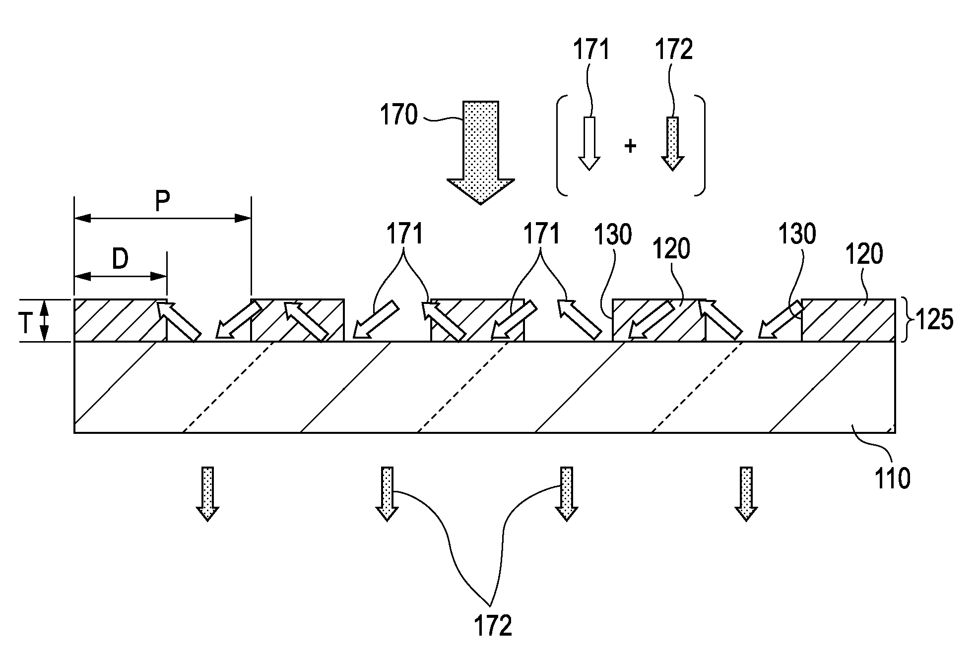
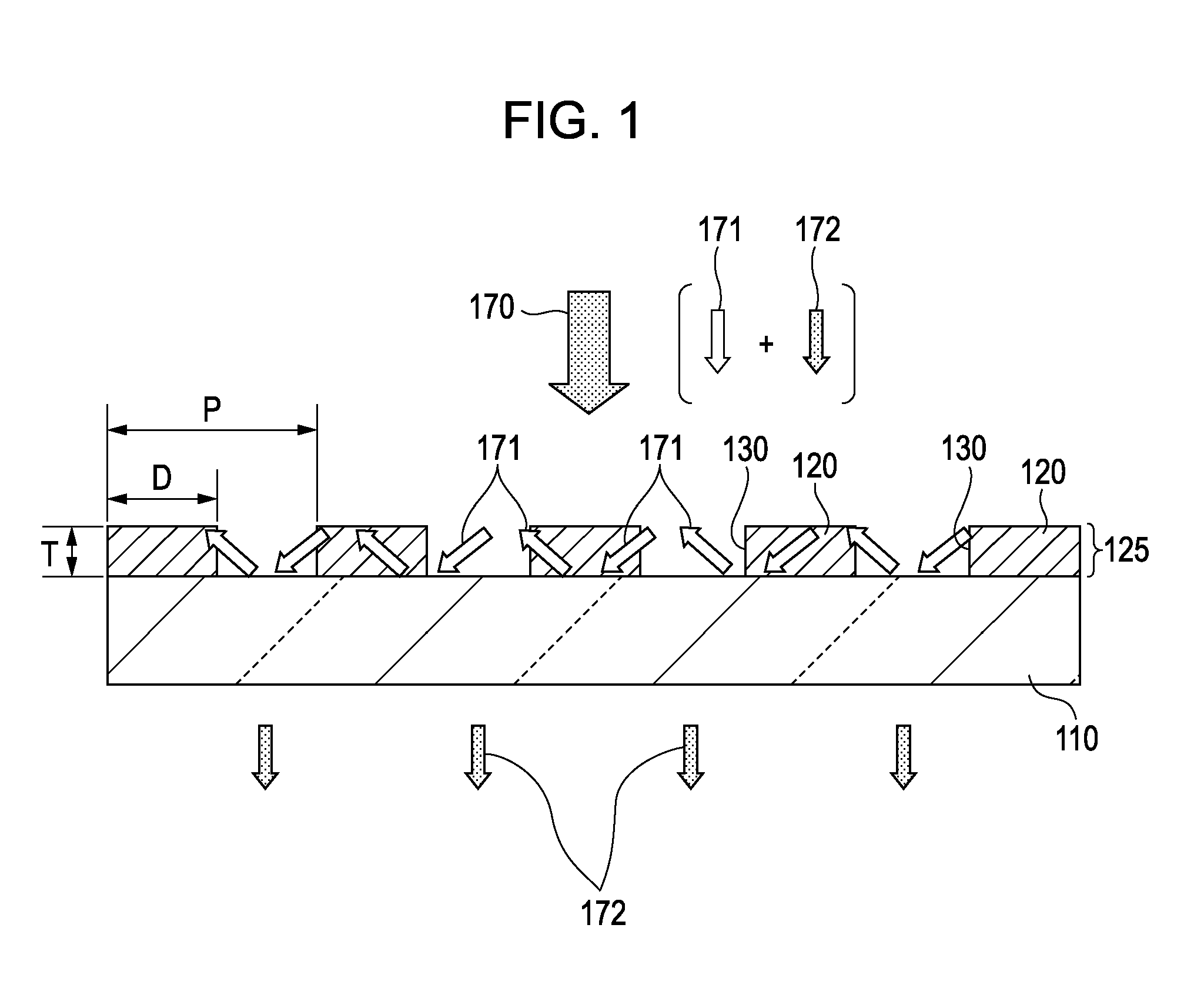
[0099]FIG. 6A shows a dielectric substrate 601 that is a quartz substrate 525 μm thick, on the surface of which a silicon layer 100 nm thick is formed as a semiconductor layer 602, on which a resist layer 603 for electron beam lithography (EB) is applied. In the case where the semiconductor layer 602 is of single crystal, the semiconductor layer 602 can be formed by preparing an SOI (Silicon On Insulator) substrate and reducing the thickness of the thin film silicon layer thereof. However, the method for forming the semiconductor layer 602 is not limited to the above, and any method known to a person of ordinary skill in the art may be used.

[0100]Next, the resist 603 is patterned using an EB lithography apparatus. A resist pattern in which squares about 140 nm on a side are arranged in a s...

second embodiment

Bayer Arrangement

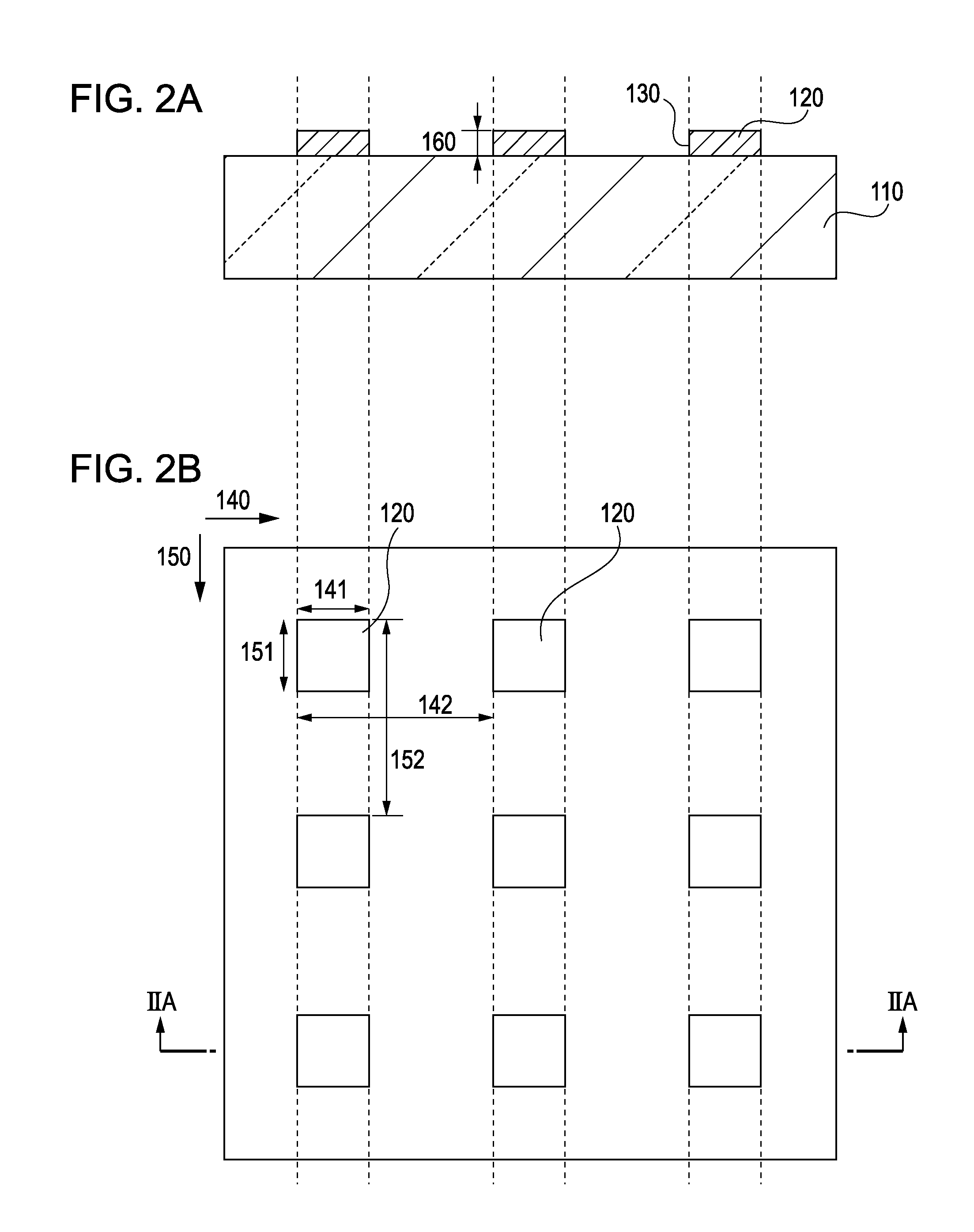
[0109]In a second embodiment, a description will be given of methods for making an RGB filter having a Bayer arrangement and the optical property of the filter. FIG. 8A shows a dielectric substrate 801 that is a quartz substrate 525 μm thick, on the surface of which a silicon layer 100 nm thick is formed as a semiconductor layer 802, on which a resist layer 803 is applied.

[0110]Next, the resist 803 is patterned using an EB lithography apparatus. A portion of the resist pattern that is about 10 μm square and in which squares about 220 nm on a side are arranged in a square lattice with a period of about 440 nm will hereinafter be referred to as a pattern portion A 804. A portion in which squares about 170 nm on a side are arranged in a square lattice with a period of about 460 nm will hereinafter be referred to as a pattern portion B 805. A portion in which squares about 140 nm on a side are arranged in a square lattice with a period of about 450 nm will hereinafter b...


PUM

PropertyMeasurementUnit
thicknessaaaaaaaaaa
transmittanceaaaaaaaaaa

Abstract

An optical filter includes a substrate, and a periodic structure in which a plurality of members formed of silicon are periodically arranged on a surface of the substrate. The filter selectively transmits light of a first wavelength included in light incident on the periodic structure in the direction of the substrate. The members are two-dimensionally arranged with a period of 400 nm to 500 nm. The dimension of the members in the direction parallel to the surface is of 120 nm to 160 nm. A local maximum value of the transmission spectrum of the first wavelength is within the range of 400 nm to 500 nm.

Description

BACKGROUND OF THE INVENTION[0001]1. Field of the Invention[0002]The present invention relates to an optical filter using guided mode resonance.[0003]2. Description of the Related Art[0004]In recent years, separately from the conventional color filter using pigment, a color filter using guided mode resonance (GMR) or Guided Resonance (GR) Mode has been proposed. The color filter using guided mode resonance takes advantage of a resonance condition between diffracted light and a waveguide mode occurring in a waveguide. Optical filters based on GMR are considered to provide high light use efficiency and a sharp resonance spectrum.[0005]Kanamori et al., in “Fabrication of Transmission Color Filters Using Silicon Subwavelength Gratings on Quartz Substrates”, IEEE Photonics Technology Letters, Vol. 18, No. 20, Oct. 15, 2006 (hereinafter referred to as Literature 1) discloses a color filter that includes a one-dimensional diffraction grating formed of silicon and uses the guided mode resona...

Claims


Application Information

Patent Timeline
Patent Type & Authority Applications(United States)
IPC IPC(8): G02F1/1335
CPCG02B5/203G02B5/1809
Inventor YAMADA, TOMOHIROKURODA, RYO
Owner CANON KK
Why Eureka
Try Eureka