Wafer level optical elements and applications thereof

Active Publication Date: 2011-01-06
NANCHANG O FILM OPTICAL ELECTRONICS TECH CO LTD
View PDF10 Cites 32 Cited by
  • Summary
  • Abstract
  • Description
  • Claims
  • Application Information

AI Technical Summary

Benefits of technology

[0012]Additionally, in some embodiments, an optical element comprising a wafer level lens further comprises one or more baffles operable to reduce amounts of stray light entering the wafer level lens. In some embodiments, an optical element comprising a wafer level lens further comprises at least one spacer coupled to the wafer leve

Problems solved by technology

One disadvantage is a reduction in modulation transfer function (MTF) values when a transparent substrate is disposed between lens structures.
Furthermore, substrate wafers contribute a significant amount to the cost of pro

Method used


Image

  • Wafer level optical elements and applications thereof
  • Wafer level optical elements and applications thereof
  • Wafer level optical elements and applications thereof

Examples


example 1

Plurality of Optical Elements

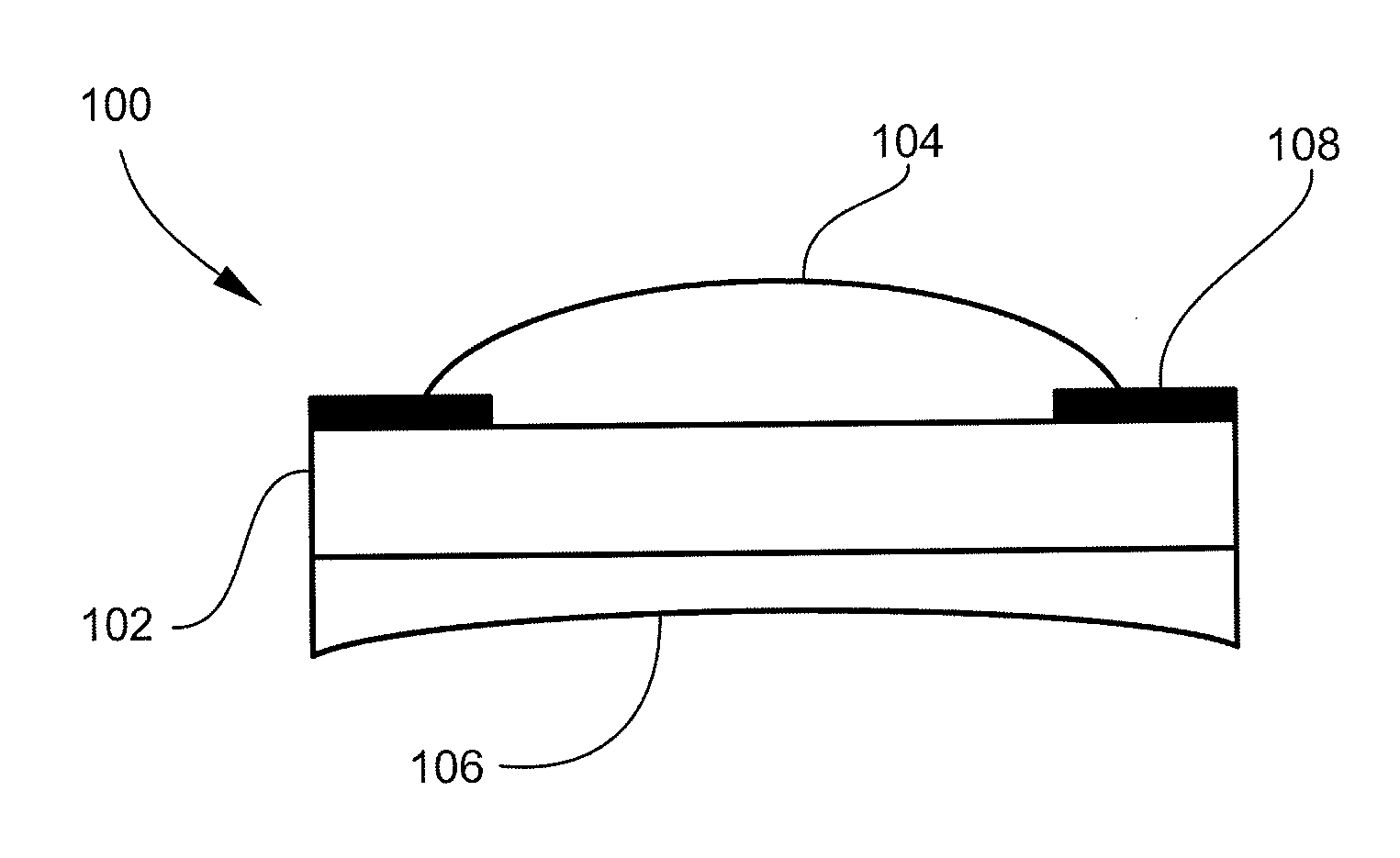
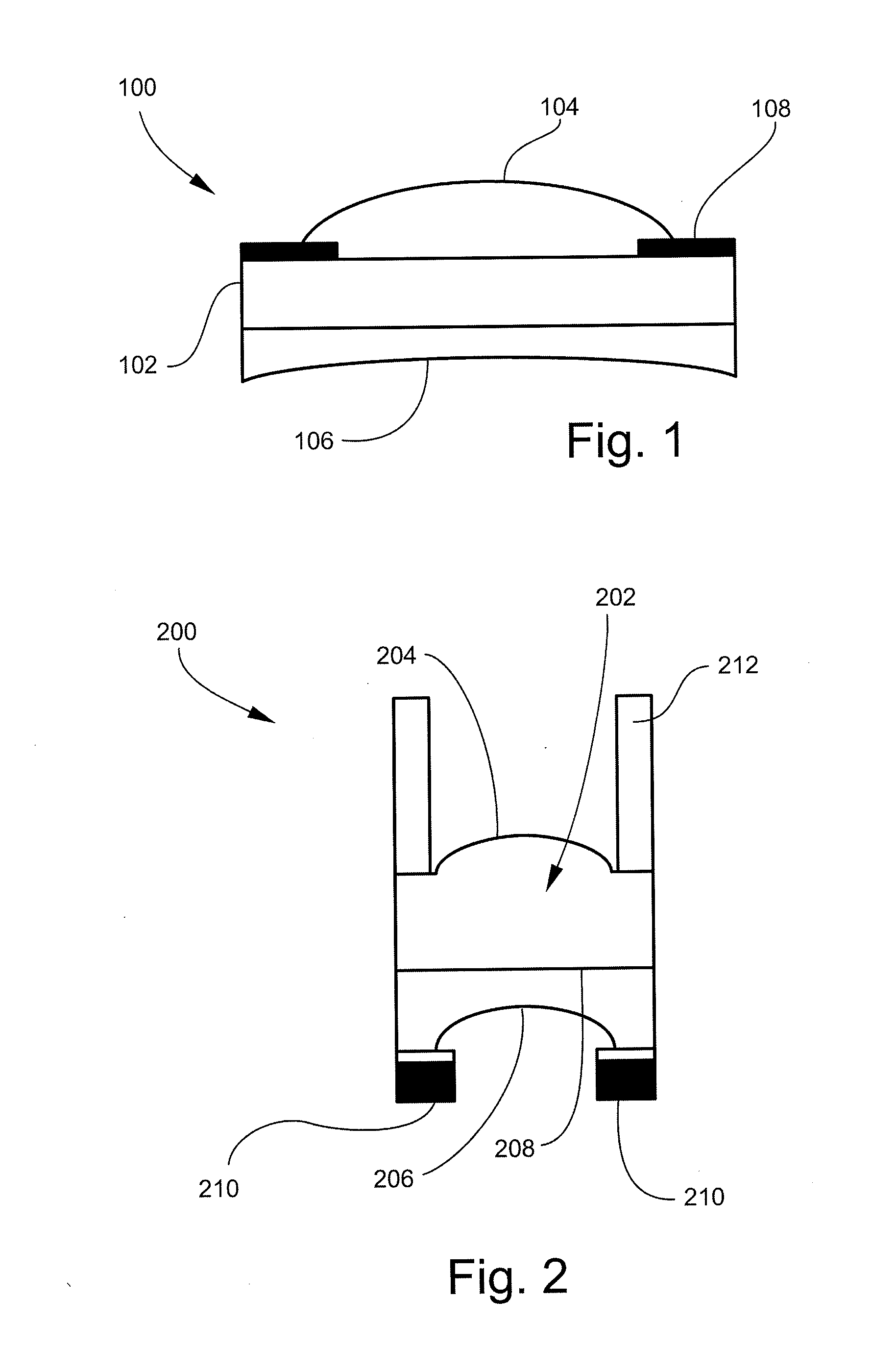
[0094]A plurality of optical elements of the present invention were fabricated according to the following procedure.

[0095]A temporary coating of polydimethylsiloxane (PDMS) was spun on temporary carrier wafer of fused silica glass at 2700 rpm followed by cure at 150° C. for 30 minutes. Optical polymer was replicated on the temporary PDMS coating to form a first wafer comprising a plurality of first lens structures. The polymer was UV-cured at 20 mW / cm2 for 50 sec. A perforated substrate was subsequently bonded to the first wafer with thermal epoxy (353ND) at 90° C. for 1 h. Afterwards, the temporary carrier wafer was separated from the first wafer.

[0096]The perforated substrate having the first lens surface above each hole was baked at 150° C. for 3 h. A layer of Cr metal having a thickness of about 500 μm was deposited on the backside of the first wafer comprising the plurality of first lens structures using thermal evaporation equipment. Positive resis...


PUM

PropertyMeasurementUnit
Polymericaaaaaaaaaa
Coefficient of linear thermal expansionaaaaaaaaaa

Abstract

The present invention provides wafer level optical elements that obviate a substrate wafer or a portion thereof disposed between optical structures or optical surfaces of the element.

Description

FIELD OF THE INVENTION[0001]The present invention relates to optical elements and, in particular, to optical elements having lens structures fabricated at the wafer level.BACKGROUND OF THE INVENTION[0002]Wafer level fabrication techniques provide for the efficient and high volume production of optical elements and other components used in optical imaging apparatus. Existing wafer level fabrication techniques for optical elements employ a transparent substrate wafer onto which optical structures, such as lenses, are formed. The transparent substrate wafer provides mechanical rigidity to the optical elements, thereby facilitating downstream handling and processing. Moreover, transparent wafer substrates provide surfaces for the installation of one or more apertures for controlling the transmission of the desired amount of electromagnetic radiation to or from other optical components or sensing components of an optical system.[0003]FIG. 1 illustrates a wafer level optical element emplo...

Claims


Application Information

Patent Timeline
IPC IPC(8): G02B11/02B32B37/02B44C1/22
CPCB29D11/00278B29D11/00365Y10T156/10G02B13/0085G02B3/0031
Inventor OVRUTSKY, DAVIDHUDDLESTON, JEREMY
Owner NANCHANG O FILM OPTICAL ELECTRONICS TECH CO LTD
Why Eureka
Try Eureka