Method of programming variable resistance element and variable resistance memory device using the same

a technology of variable resistance and memory device, which is applied in the direction of digital storage, semiconductor devices, instruments, etc., can solve the problems of limiting the current attempt at more microfabricated flash memory using floating gates to meet such requirements, and achieve stable and high-speed operations, high speed, and high speed

Active Publication Date: 2011-01-06
PANASONIC SEMICON SOLUTIONS CO LTD
View PDF14 Cites 20 Cited by
  • Summary
  • Abstract
  • Description
  • Claims
  • Application Information

AI Technical Summary

Benefits of technology

[0034]The method of programming a variable resistance element according to the present invention can change a resistance of a variable resistance film with stability and at a high speed, which enables the variable resistance element to perform stable and high-speed operations. In addition, the variable resistance memory device employing the method according to the present invention also enables the variable resistance film to change the resistance with stability and at a high speed.

Problems solved by technology

It is considered that current attempt at more microfabricated flash memories using floating gates has a limit to satisfy such requirements.

Method used


Image

  • Method of programming variable resistance element and variable resistance memory device using the same
  • Method of programming variable resistance element and variable resistance memory device using the same
  • Method of programming variable resistance element and variable resistance memory device using the same

Examples


first embodiment

Variation of First Embodiment

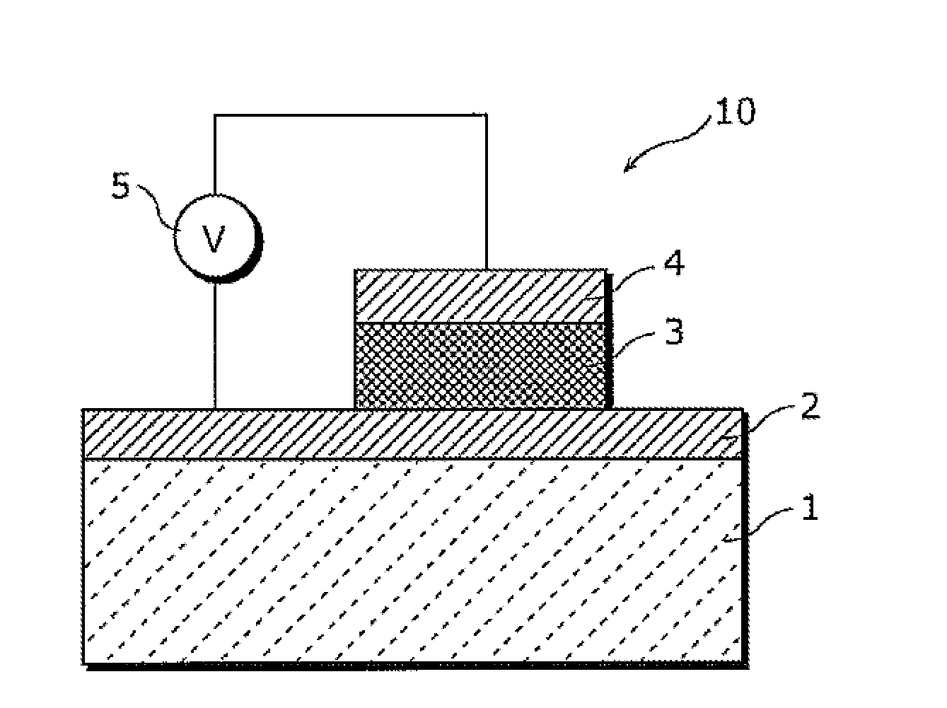
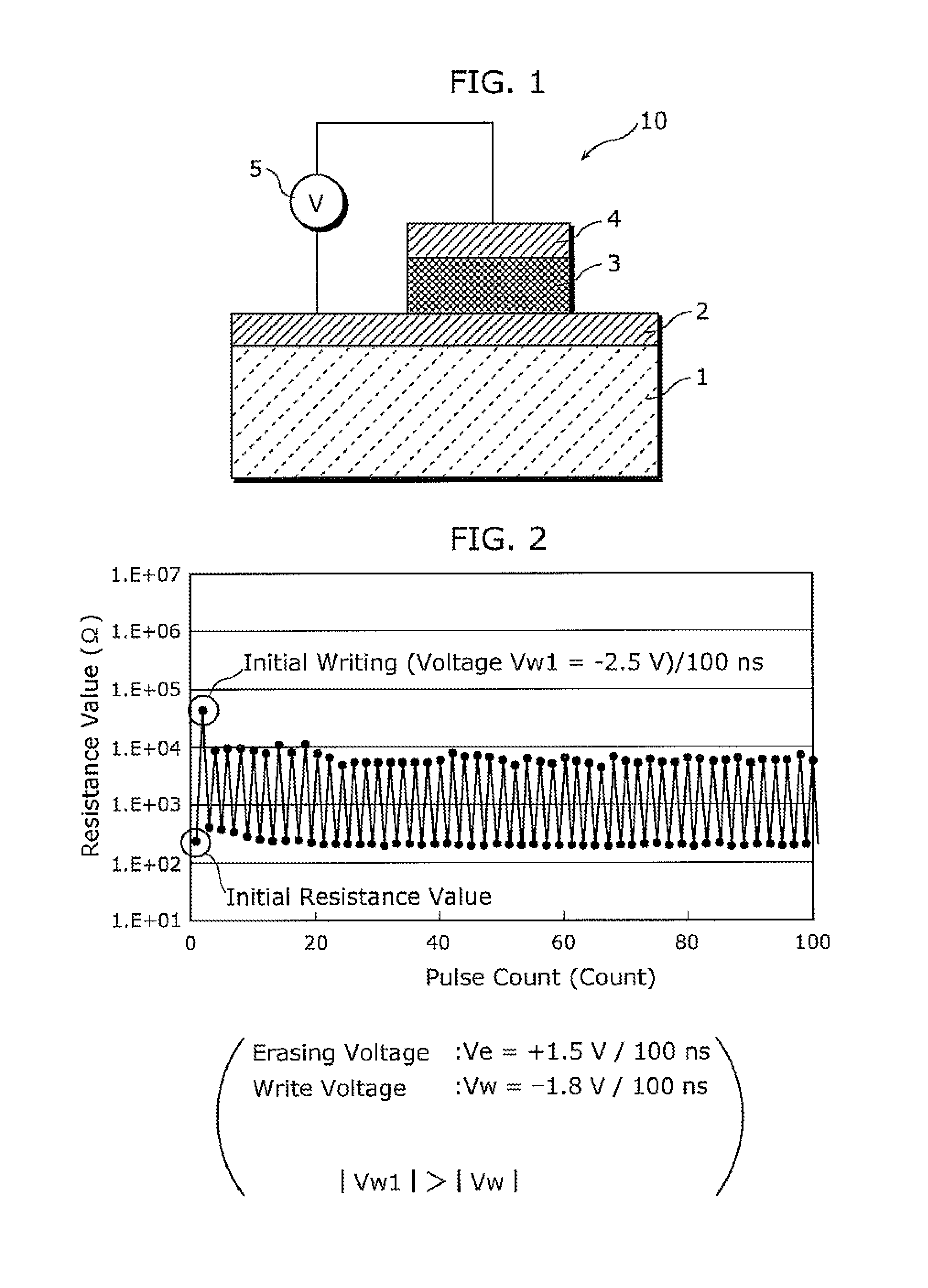
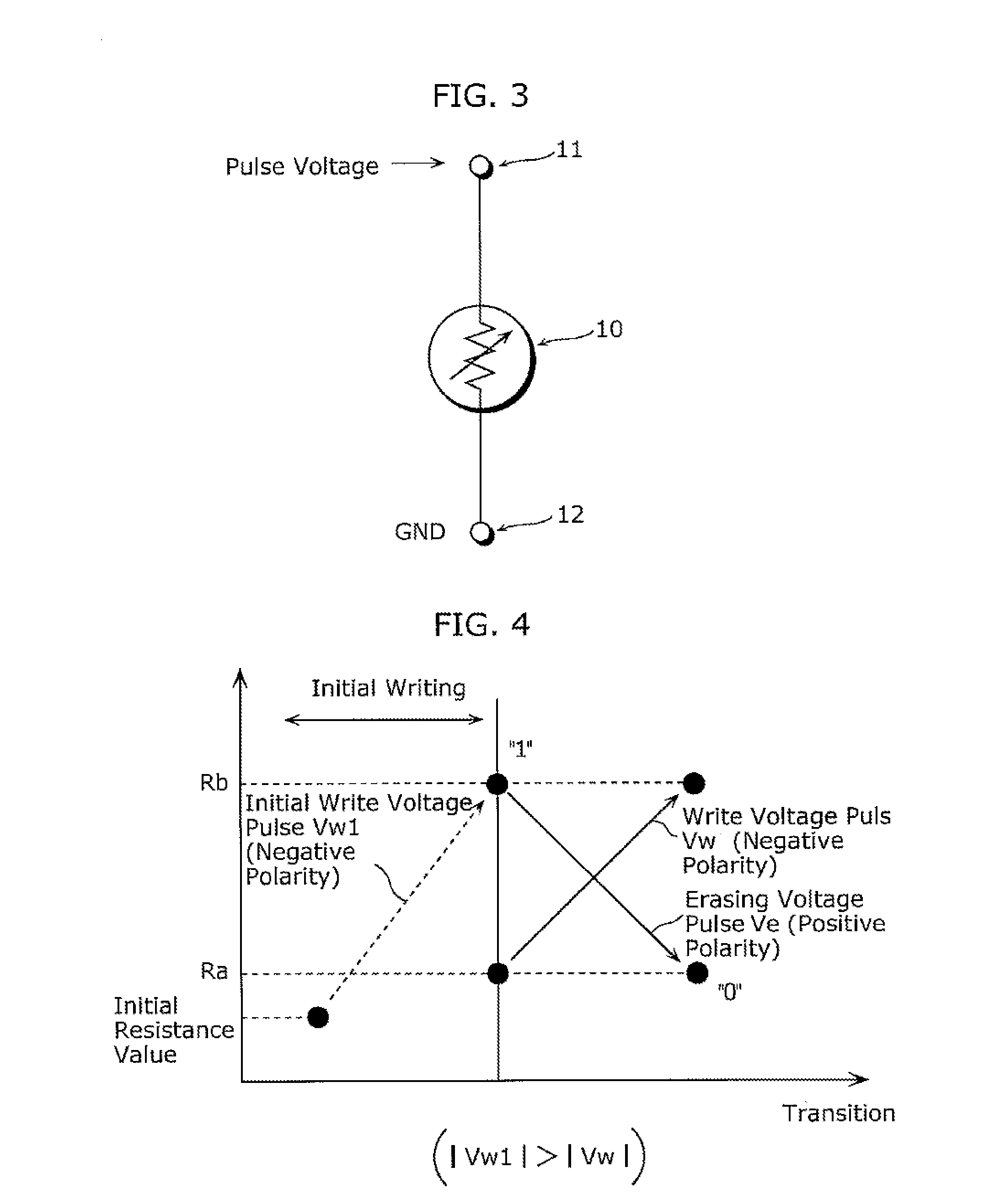
[0114]It should be noted that the voltage value Vw1 and the pulse width of the initial write voltage pulse, the voltage value Vw and the pulse width of the subsequent write voltage pulse, the voltage value Ve and the pulse width of the erasing voltage pulse, and the value of the readout voltage are not limited to the above-described values. They may be any values as far as a relationship between voltages satisfies |Vw1|>|Vw| and the values are suitable for variable resistance elements actually manufactured.

[0115]It is also possible that another layer is formed between the lower electrode 2 and the variable resistance layer 3 or between the variable resistance layer 3 and the upper electrode 4. The structure may be modified as far as the lower electrode 2 and the variable resistance layer 3 are electrically connected to each other and the variable resistance layer 3 and the upper electrode 4 are electrically connected to each other.

[0116]As described earl...

first example

[0119]On the silicon substrate, the lower electrode made of platinum (Pt) (with dimensions of 10 μm×10 μm) is formed by a sputtering method to have a thickness of 0.1 μm. Then, a Ta target is prepared, and oxygen gas is mixed to argon gas according to a predetermined ratio of flow rates so as to perform reactive sputtering for the Ta target. Thereby, the variable resistance layer 3 comprising a tantalum oxide represented by the chemical formula of TaOx is formed on the lower electrode 2. The variable resistance layer is manufactured at ambient temperature without heating the substrate, for example. Then, on the variable resistance layer, the upper electrode made of Pt is formed by a sputtering method to have a thickness of 0.1 μm. A mask and photolithography are used for etching the variable resistance layer and the upper electrode together. Thereby, the variable resistance element is manufactured. Each of the upper electrode and the variable resistance layer has dimensions of 0.5 μ...

second example

[0133]Most of variable resistance elements used in the first example show resistance variation with good endurance characteristics. However, there are exceptionally rare variable resistance elements that fail writing to change a low resistance state to a high resistance state. In order to solve the drawbacks, the second example includes a determination step for examining a resistance state of the variable resistance element 10 after writing, in addition to the processing in the first example. If writing fails, a re-write voltage pulse (with a voltage value Vw2) satisfying a relationship |Vw2|>|Vw| is applied to perform re-writing. Then, the general subsequent write voltage pulses (with the voltage value Vw) and the erasing voltage pulse (with the voltage value Ve) are applied.

[0134]FIG. 13 shows a variation of a resistance value of the variable resistance layer in the case where the voltage value Vw1 of the initial write voltage pulse is set to be −2.5V (with a pulse width of 100 ns...


PUM


Abstract

A method of programming a variable resistance element to be operated with stability and at a high speed is provided. The method programs a nonvolatile variable resistance element (10) including a variable resistance layer (3), which changes between a high resistance state and a low resistance state depending on a polarity of an applied electric pulse, and a lower electrode (2) and an upper electrode (4). The method includes: writing steps (S11) and (S15) to cause the variable resistance layer (3) to change from the low resistance state to the high resistance state by applying a write voltage pulse; and an erasing step (S13) to cause the variable resistance layer (3) to change from the high resistance state to the low resistance state. In the writing steps, a write voltage pulse is applied between the electrodes so as to satisfy |Vw1|>|Vw| where Vw1 represents a voltage value of the write voltage pulse in the first writing step (S11) after manufacturing the variable resistance element (10) and Vw represents a voltage value of the write voltage pulse in writing steps after the first writing step (S15) after manufacturing the variable resistance element (10).

Description

TECHNICAL FIELD[0001]The present invention relates to methods of programming a variable resistance element. More particularly, the present invention relates to a method of programming a variable resistance element having electrical resistance that varies depending on applied electric pulses, and a variable resistance memory device using the method.BACKGROUND ART[0002]With the development of digital technologies regarding electronic devices, in order to store data such as images, requirements arise for a larger capacity of nonvolatile variable resistance elements, reduction of power consumption for writing, a higher speed for a writing / reading time, a longer duration, and the like. It is considered that current attempt at more microfabricated flash memories using floating gates has a limit to satisfy such requirements.[0003]One conventional technology having a possibility of satisfying the requirements is disclosed to provide a nonvolatile variable resistance element made of a perovs...

Claims


Application Information

Patent Timeline
Patent Type & Authority Applications(United States)
IPC IPC(8): G11C11/00
CPCG11C13/0007G11C13/0069G11C2013/0083G11C2013/009H01L45/1675H01L45/04H01L45/1233H01L45/146H01L45/1625H01L27/101H10N70/20H10N70/826H10N70/8833H10N70/026H10N70/063
Inventor MURAOKA, SHUNSAKUTAKAGI, TAKESHISHIMAKAWA, KAZUHIKO
Owner PANASONIC SEMICON SOLUTIONS CO LTD
Why Eureka
Try Eureka