Optical display device manufacturing system and optical display device manufacturing method

a technology of optical display device and manufacturing system, which is applied in the direction of mechanical control device, process and machine control, instruments, etc., can solve the problem of increasing production cos

Inactive Publication Date: 2011-01-13
NITTO DENKO CORP
View PDF1 Cites 10 Cited by
  • Summary
  • Abstract
  • Description
  • Claims
  • Application Information

AI Technical Summary

Benefits of technology

[0019]According to the present invention, the detection condition of the defect in the inspection of the optical film before being bonded to the optical display unit carried out by the optical film inspection means is corrected based on the result of inspection of the optical display device with the optical film bonded, carried out by the optical display device inspection means, and the optical film including the defect detected by the optical film inspection means based on the corrected detection condition is rejected. Accordingly, since it is possible to adjust the standard of the defect inspection carried out by the optical film inspection means in conformity to the standard of the defect inspection which is later carried out by the optical display device inspection means, it is possible to more preferably carry out the defect inspection, and to improve a yield ratio of the optical display device.
[0022]According to the present invention, it is possible to cut the optical film while avoiding the defect portion in such a manner as to prevent the defect detected by the optical film inspection means based on the corrected detection condition from being included within the region bonded to the optical display unit, and to reject the optical film including the defect and being cut. Accordingly, since it is possible to efficiently reject the portion including the defect of the optical film, it is possible to more improve the yield ratio of the optical film.
[0027]According to the present invention, in the case that the defect which is detected by the optical film inspection means is not detected by the optical display device inspection means, the condition corresponding to the defect is excluded from the detection condition of the optical film inspection means. Accordingly, even in the case that the standard of the defect inspection before the bonding carried out by the optical film inspection means is higher than the standard of the defect inspection after the bonding carried out by the optical display device inspection means, it is possible to prevent a minor defect in such a level that is not detected as the defect in the defect inspection after the bonding from being over detected by the defect inspection before the bonding. Accordingly, it is possible to further preferably carry out the defect inspection.
[0035]According to the present invention, an optical display device manufacturing method producing the same effects as the optical display device manufacturing system according to the first aspect of the present invention can be provided.
[0038]According to the present invention, an optical display device manufacturing method producing the same effects as the optical display device manufacturing system according to the second aspect of the present invention can be provided.
[0040]According to the present invention, an optical display device manufacturing method producing the same effects as the optical display device manufacturing system according to the third aspect of the present invention can be provided.

Problems solved by technology

However, there are a problem of a production cost increase caused by multiple steps, a problem of the scratch, the dust, the dirt and the like generated by the multiple steps and the transport, a necessity of the inspection step caused thereby, and a problem that it is necessary to store and manage many kinds of sheet materials as a stock.

Method used


Image

  • Optical display device manufacturing system and optical display device manufacturing method
  • Optical display device manufacturing system and optical display device manufacturing method
  • Optical display device manufacturing system and optical display device manufacturing method

Examples


first embodiment

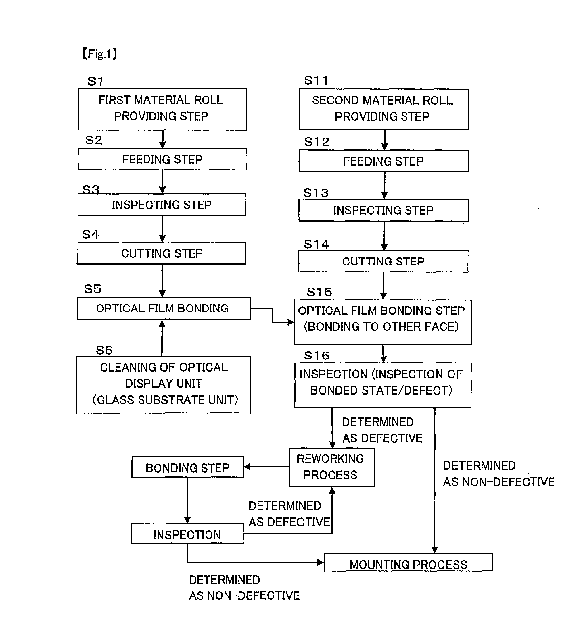
[0053]A description will be given below of a first embodiment in accordance with the present invention. FIG. 1 shows a flow chart of a production method of an optical display device in accordance with the first embodiment. A production system in accordance with the first embodiment corresponds to a construction example which is not provided with first and second pre-inspection peeling apparatuses, and first and second release film laminating apparatuses in a structure of a production system in accordance with a second embodiment mentioned below. Further, a construction which is not provided with first and second defect inspection apparatuses, can be exemplified as the other embodiment of the production system in accordance with the first embodiment.

[0054](Optical Display Unit)

[0055]First, for example, a glass substrate unit of a liquid crystal cell, an organic electroluminescent (EL) light-emitting unit and the like can be listed up, as an optical display unit used in the present in...

second embodiment

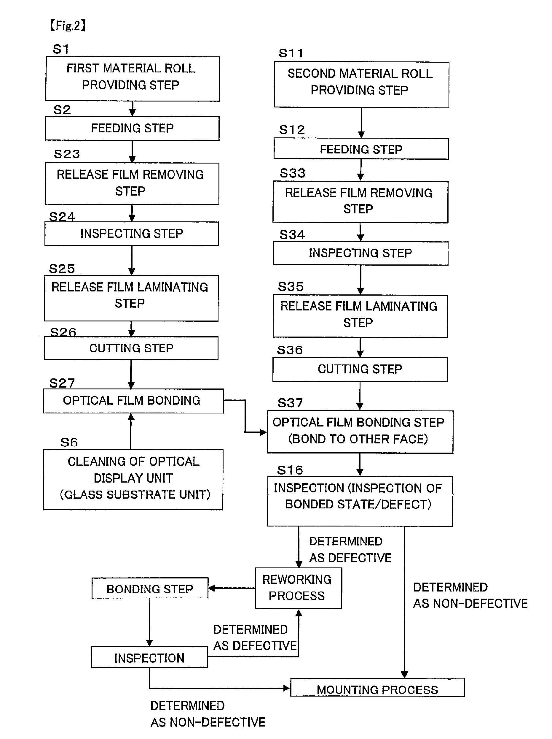
[0081]A description will be given below of the second embodiment in accordance with the present invention. FIG. 2 shows a flow chart of a production method of an optical display device in accordance with the second embodiment. The same steps as those of the first embodiment will be described briefly.

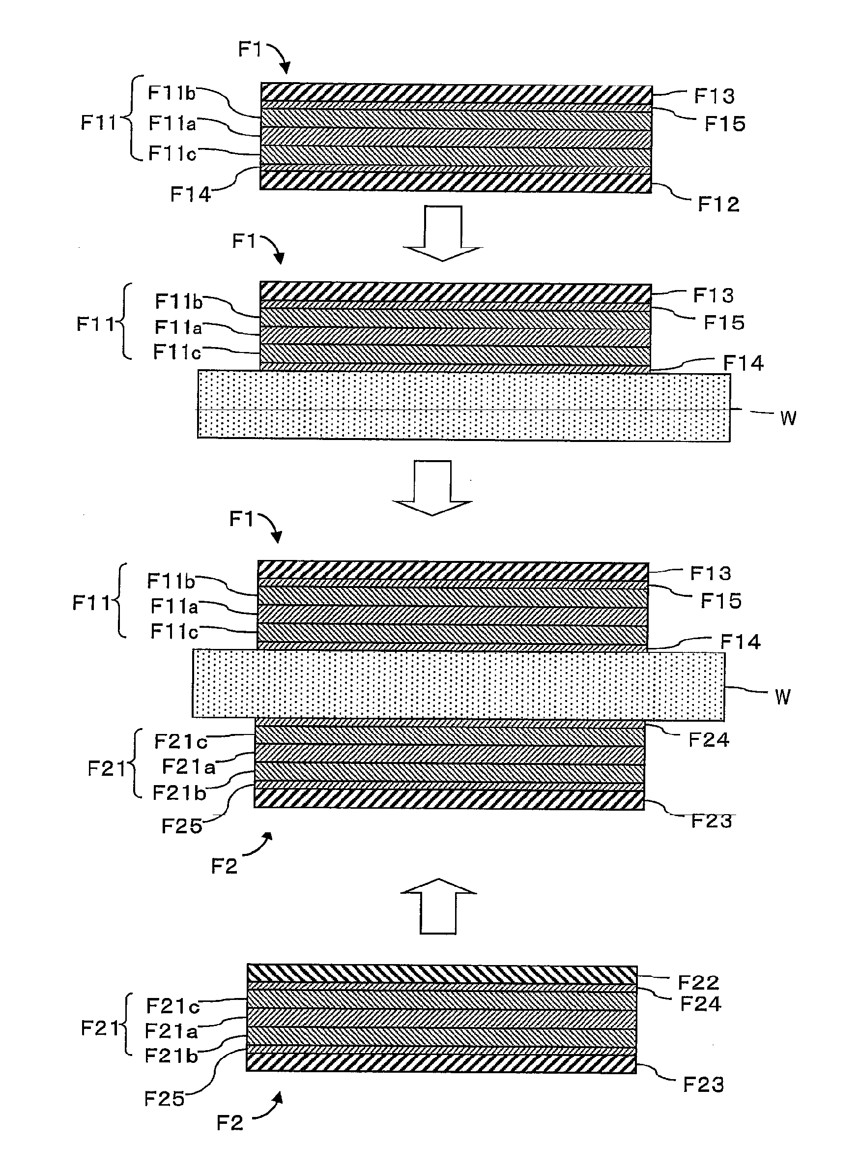
[0082](1) First Material Roll Providing Step (S1 in FIG. 2). A long first sheet material F1 is provided as a first material roll. A lamination structure of a first sheet material F1 is the same as that of the first embodiment shown in FIG. 3.

[0083](2) Feeding Step (S2 in FIG. 2). The first sheet material F1 is unwound from the provided and placed first material roll, and is fed to a downstream side.

[0084](3) Release Film Removing Step (S23 in FIG. 2). A first pre-inspection peeling apparatus peels off the first release film F12 from the fed first sheet material F1. Details of the peeling mechanism will be mentioned below.

[0085](4) First Inspecting Step (S24 in FIG. 2: Optical Film Inspec...


PUM

PropertyMeasurementUnit
sizeaaaaaaaaaa
optical film inspectionaaaaaaaaaa
opticalaaaaaaaaaa

Abstract

Provided are an optical display device manufacturing system and an optical display device manufacturing method which can more preferably carry out a defect inspection. A detection condition of a defect in the inspection of an optical film before being bonded to an optical display unit carried out by a defect inspection apparatus (14, 24) is corrected based on the result of inspection of the optical display device with the optical film bonded, carried out by an inspection apparatus (30), and the optical film including the defects detected by the defect inspection apparatuses (14, 24) based on the corrected detection condition are excluded. Accordingly, since it is possible to adjust the standard of the defect inspection carried out by the defect inspection apparatus (14, 24) in conformity to the standard of the defect inspection which is later carried out by the inspection apparatus (30), it is possible to more preferably carry out the defect inspection, and it is possible to improve a yield ratio of the optical film.

Description

TECHNICAL FIELD[0001]The invention relates to an optical display device manufacturing system and an optical display device manufacturing method for manufacturing an optical display device by delivering an optical film from a material roll formed by winding the optical film into a roll shape, and cutting the optical film into a predetermined size so as to be bonded to an optical display unit.BACKGROUND ART[0002]A production method of an optical display device mounted to a conventional liquid crystal display device is conceptually shown in FIG. 7. First in an optical filmmaker, a step produces a long (web-like) sheet material having an optical film as a material roll (#1). The concrete production step is a known production step, and a description thereof will not be given. As the long (web-like) sheet material, for example, there are a polarizing plate material, a retardation plate material, a laminated film material of the polarizing plate and the retardation plate, and the like whic...

Claims


Application Information

Patent Timeline
Patent Type & Authority Applications(United States)
IPC IPC(8): B32B41/00
CPCB32B41/00B32B2307/40G02F1/1303G02F1/1309C09J7/0207G02F2202/28B29D11/00644B29D11/0073G02F1/133528C09J7/38
Inventor KITADA, KAZUOYURA, TOMOKAZUKOSHIO, SATORUNAKAZONO, TAKUYA
Owner NITTO DENKO CORP
Why Eureka
Try Eureka