
Tft, shift register, scan signal line driving circuit, and display device

Inactive Publication Date: 2011-01-13
SHARP KK
View PDF12 Cites 22 Cited by
  • Summary
  • Abstract
  • Description
  • Claims
  • Application Information

AI Technical Summary

Benefits of technology

[0015]The conventional TFT provided with a bootstrap capacitor requires being large in size so that the TFT body section secures a large channel width, as described previously. Therefore, it is inevitable that manufacturing of TFTs with low yield seriously decreases a proportion of non-defective panels obtained. However, with increase of a load connected to an output of a TFT including the bootstrap capacitor, a capacitance value required for the bootstrap capacitor to obtain a satisfactory bootstrap effect increases. Accordingly, the bootstrap capacitor occupies a large area on a panel.

Problems solved by technology

Therefore, it is inevitable that manufacturing of TFTs with low yield seriously decreases a proportion of non-defective panels obtained.
This results in extremely large picture frame size of the display device.
Thus, the conventional TFT provided with a bootstrap capacitor has the problem that a footprint of the bootstrap capacitor is extremely large.

Method used


Image

  • Tft, shift register, scan signal line driving circuit, and display device
  • Tft, shift register, scan signal line driving circuit, and display device
  • Tft, shift register, scan signal line driving circuit, and display device

Examples


Embodiment Construction

[0075]The following will describe one embodiment of the present invention with reference to FIGS. 1 through 6.

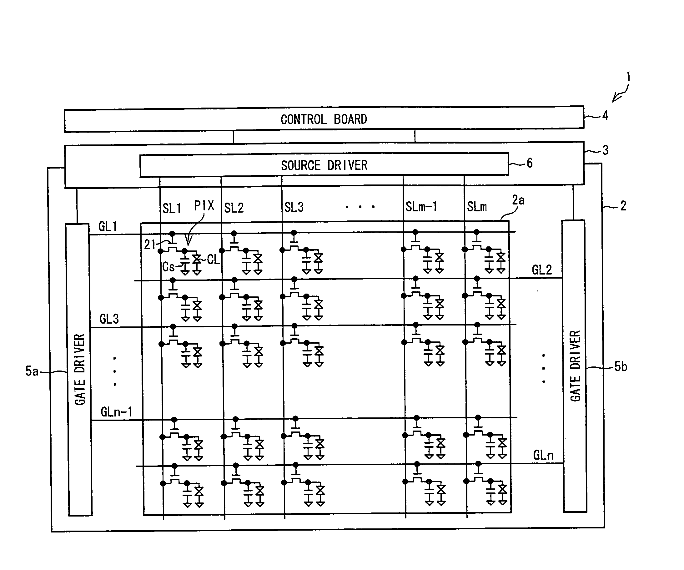
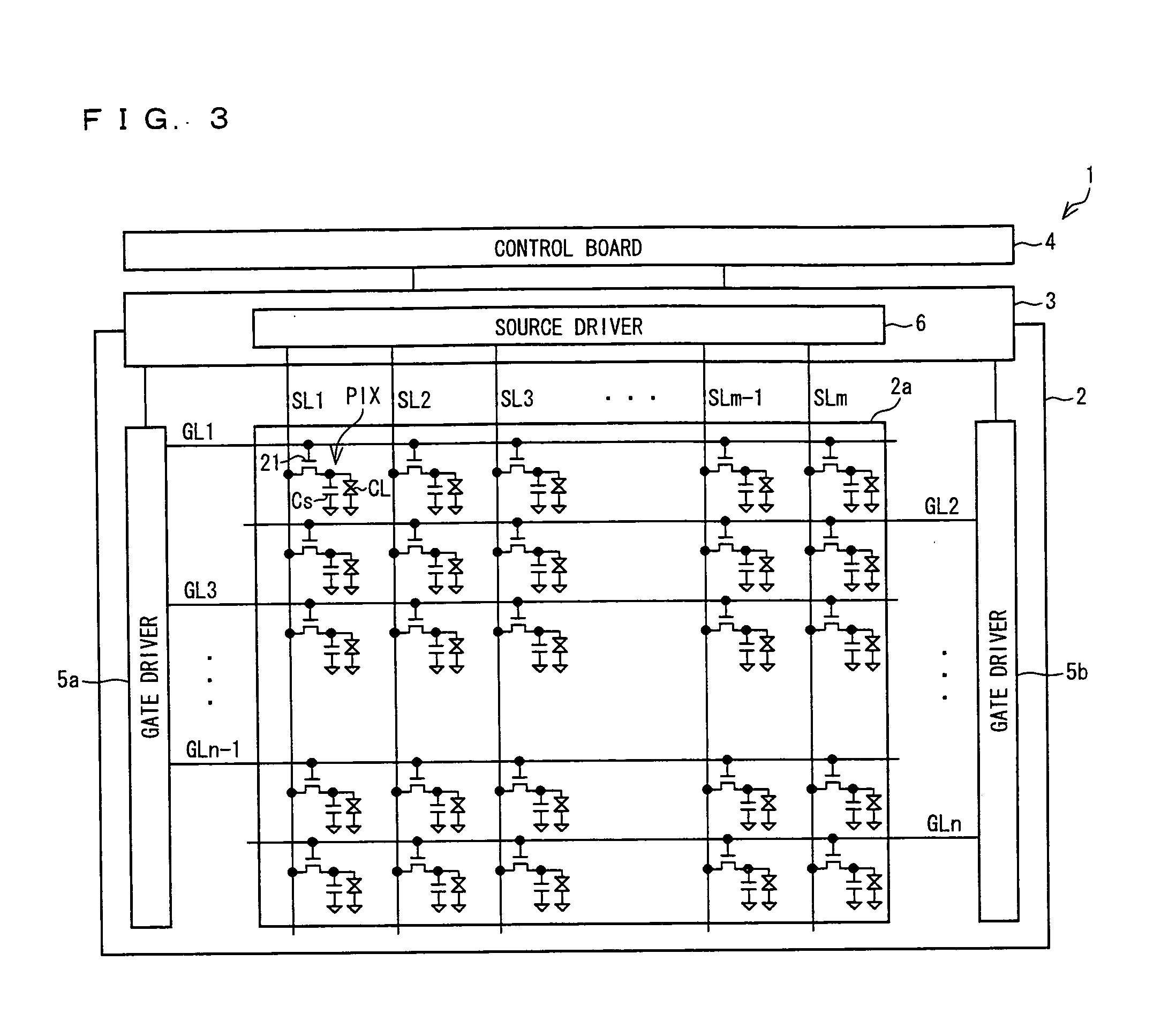
[0076]FIG. 3 shows the configuration of a liquid crystal display device 1 that is a display device according to the present embodiment.

[0077]The liquid crystal display device 1 includes a display panel 2, a flexible printed circuit board 3, and a control board 4.

[0078]The display panel 2 is an active matrix display panel arranged such that, using amorphous silicon, polycrystalline silicon, CG silicon, microcrystalline silicon, or the like silicon, a display region 2a, a plurality of gate bus lines GL, a plurality of source bus lines SL, and gate drivers 5a and 5b are built onto a glass substrate. The display region 2a is a region where a plurality of pixels PIX are arranged in a matrix manner. Each of the pixels PIX includes a TFT 21 that is a selection element of the pixel, a liquid crystal capacitor CL, and an auxiliary capacitor Cs. A gate of the TFT 21 is connected to th...


PUM


Abstract

A TFT includes, in at least one embodiment, a capacitor formed: so as to have a region where a first capacitor electrode connected to a source electrode and a second capacitor electrode connected to a gate electrode are arranged to be stacked in a thickness direction and mutually opposed across a first dielectric layer therebetween; and so as to have a region where the first capacitor electrode and a third capacitor electrode connected to the gate electrode are arranged to be stacked in the thickness direction and mutually opposed across a second dielectric layer therebetween with a coupling between the first capacitor electrode and the third capacitor electrode and a coupling between the first capacitor electrode and the second capacitor electrode formed over mutually opposite faces of the first capacitor electrode. This realizes a TFT which can save a footprint of a capacitor connected to a TFT body section.

Description

TECHNICAL FIELD[0001]The present invention relates to a TFT including a capacitor that is added between a gate and a source.BACKGROUND ART[0002]In recent years, monolithic integration of a gate driver has been developed for the purpose of cost reduction. In the monolithic integration, the gate driver is formed from amorphous silicon on a liquid crystal panel. The term “monolitic gate driver” is also associated with the terms such as “gate driver-free”, “built-in gate driver in panel”, and “gate in panel”. For example, Patent Literature 1 discloses shift registers of monolithic gate drivers.[0003]FIG. 7 shows circuit configuration of each shift register stage disclosed in Patent Literature 1.[0004]The following describes essential structure and operations of this circuit. FIG. 11 shows the structure of an n-th stage of shift register stages cascaded with each other. To an input terminal 12, a gate output from a preceding stage is supplied. This supply causes an output transistor 16 t...

Claims


Application Information

Patent Timeline
IPC IPC(8): G09G5/00H01L33/08H01L33/16
CPCG02F1/1368G09G3/3677H01L27/124H01L27/1255G09G2310/0286
Inventor KIKUCHI, TETSUOTANAKA, SHINYAIMAI, HAJIMEKITAGAWA, HIDEKIYAMASAKI, CHIKAOKATAOKA, YOSHIHARU
Owner SHARP KK
Features
  • Generate Ideas
  • Intellectual Property
  • Life Sciences
  • Materials
  • Tech Scout
  • Unparalleled Data Quality
  • Higher Quality Content
  • 60% Fewer Hallucinations
Learn More