Semiconductor device with large blocking voltage and manufacturing method thereof

a technology of blocking voltage and semiconductor, applied in the direction of semiconductor devices, basic electric elements, electrical appliances, etc., can solve the problems of low channel mobility and no effective measures to reduce threshold voltage, and achieve the effect of reducing threshold voltage, low threshold voltage, and large channel mobility

Inactive Publication Date: 2011-01-27
HITACHI LTD
View PDF3 Cites 43 Cited by
  • Summary
  • Abstract
  • Description
  • Claims
  • Application Information

AI Technical Summary

Benefits of technology

[0046]This invention is capable of maintaining a low threshold voltage by setting a p body region concentration of 2×1017 cm−3 or less, and further capable of maintaining the blocking voltage with no punch-through between the source and drift regions by making the width of the p body region narrower than the p body region depth (channel length). Moreover, by making the p body region width narrower than the sum of depletion layer widths (maximum depletion layer width) from channels on both sides in an inverted state, the p body region can be fully depleted until an inverted layer is attained, and the threshold voltage lowered even further.
[0047]The present invention is capable of rendering a semiconductor power device containing UMOSFET possessing large channel mobility and whose threshold voltage can be lowered with no loss in blocking voltage.

Problems solved by technology

Problems with the background art as described above when attempting to form a UMOSFET are therefore that the channel mobility is low, and currently there are no effective measures for lowering the threshold voltage without causing a drop in the blocking voltage.

Method used


Image

  • Semiconductor device with large blocking voltage and manufacturing method thereof
  • Semiconductor device with large blocking voltage and manufacturing method thereof
  • Semiconductor device with large blocking voltage and manufacturing method thereof

Examples


first embodiment

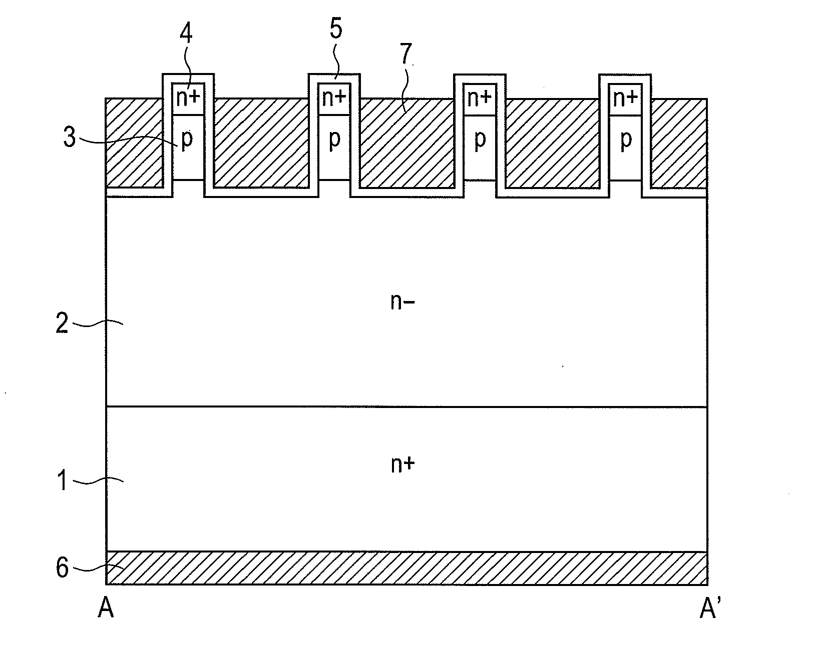
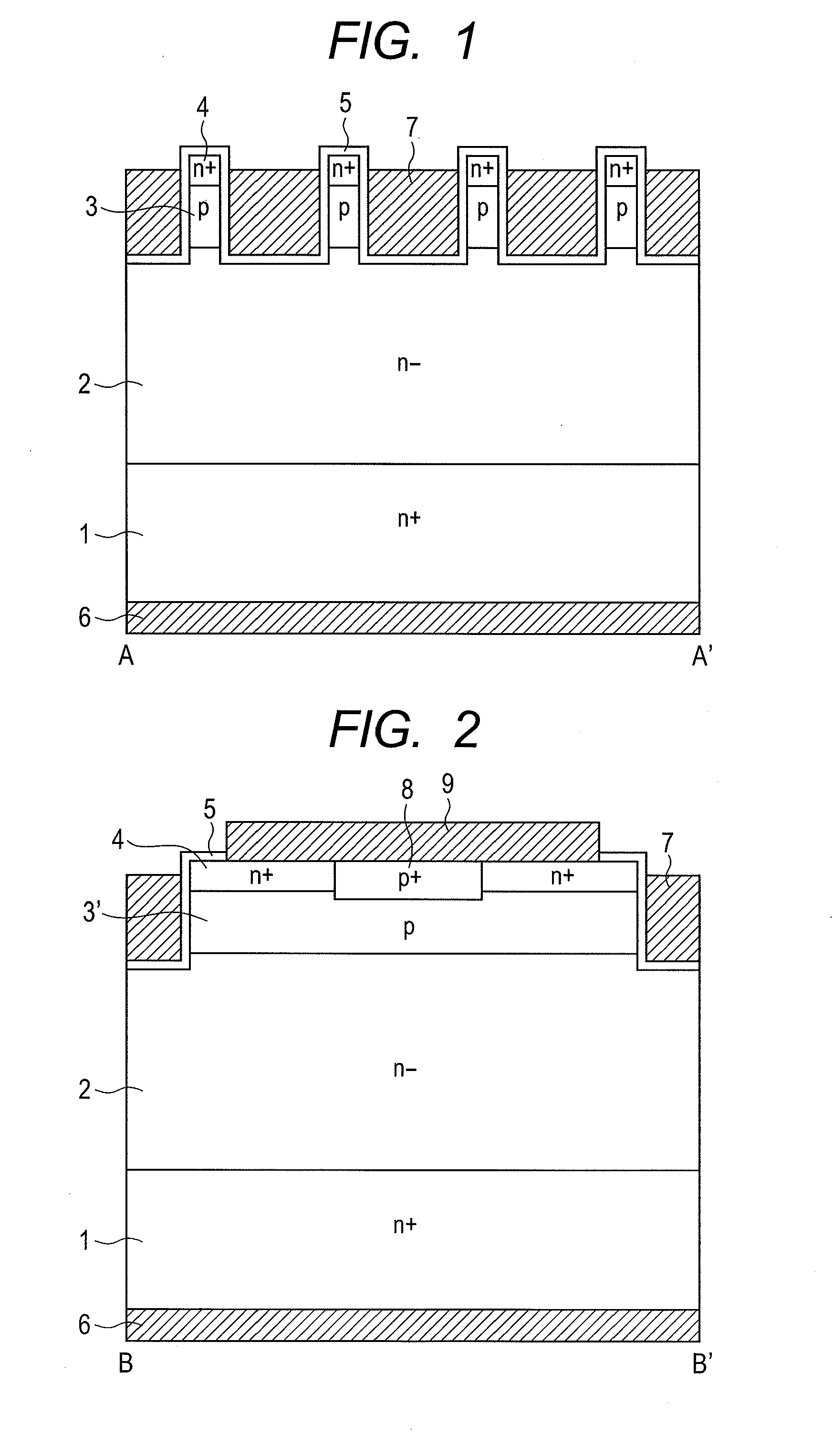
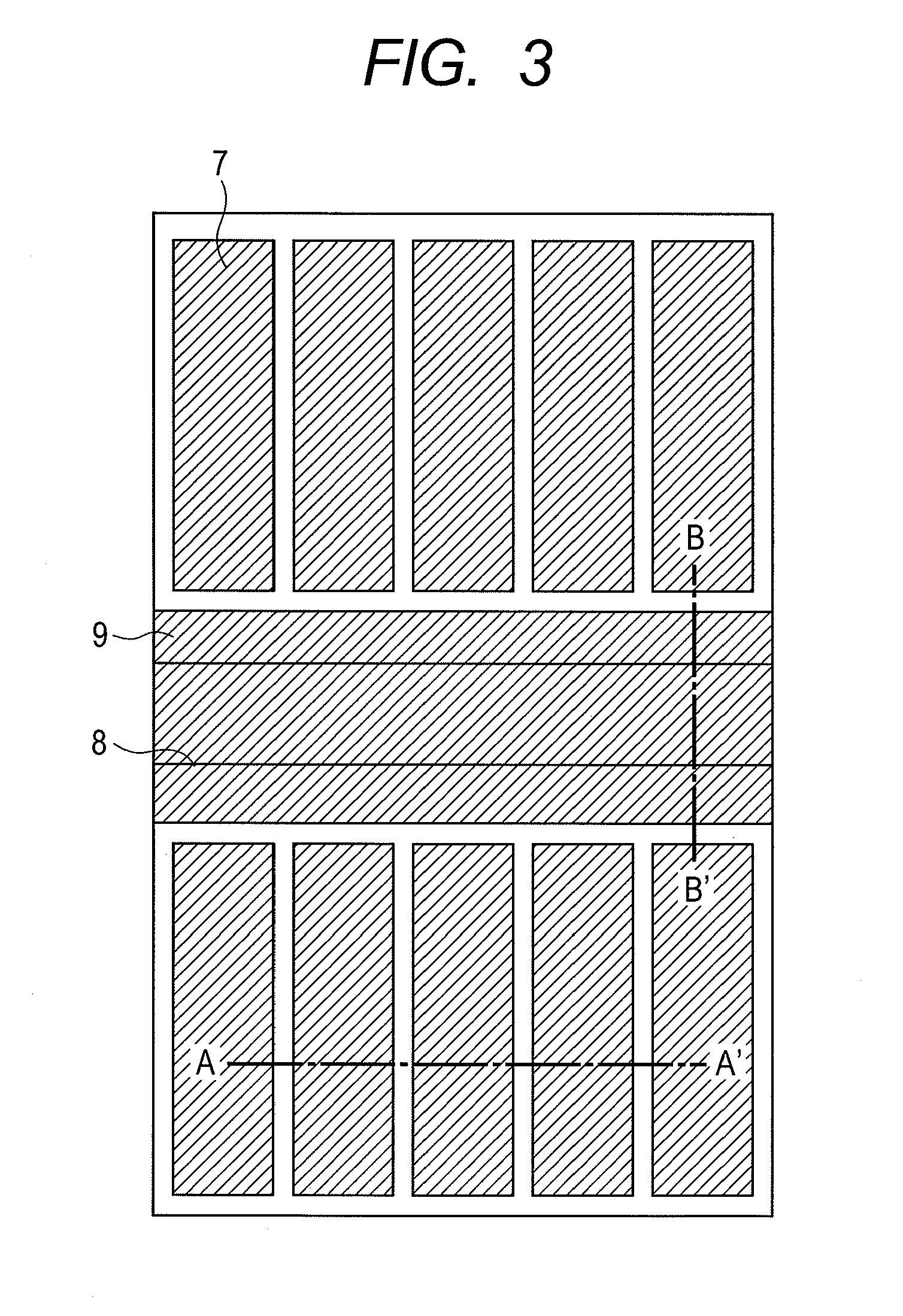
[0063]The embodiments of this invention are described next while referring to the drawings. FIG. 1 and FIG. 2 are drawings showing the cross sectional structure of the UMOSFET of this invention. FIG. 3 is a drawing showing a flat layout view of the UMOSFET of this invention. The section taken along lines A-A′ in FIG. 3 is the same cross section in FIG. 1; and the section taken along lines B-B′ is the same cross section as in FIG. 2. A drift region 2 for the n− epitaxial layer is formed on the drain region 1 of the n+ substrate formed from silicon carbide as the base material. A p body region 3 and an n+ source region 4 are respectively formed on the drift region 2, and trenches are formed so as to pierce through the n+ source region 4 and the p body region 3. A gate insulating film 5 made from oxidized film is formed on the upper section of the source region 4 and of the bottom and side walls of the trench; and a gate electrode 7 is embedded within the trench via this gate insulatin...

second embodiment

[0075]FIG. 14 shows a cross sectional structural view of the second embodiment. The second embodiment differs from the first embodiment in the point that due to channel doping, the channel concentration is lower than the p body region 3 concentration near the trench side walls. Forming a channel layer 10 with a concentration lower than the p body region 3 allows using a lower threshold voltage than the first embodiment and also allows raising the current density.

[0076]The fabrication process for the present embodiment is basically the same as the first embodiment and differs only in the point that the channel layers were formed by sloped ion implantation after forming the trenches. The condition for sloped ion implantation was 15 keV at a dosage of 5×1011 cm−2. All other design values were the same as the first embodiment. Channel doping was used to form channel layers of 5×1016 cm−3 at a width of approximately 50 nm from the trench side walls. Special characteristics were a drop in...

third embodiment

[0077]The third embodiment of this invention is described next utilizing the device planar structural view shown in FIG. 15. The point where this embodiment differs from the first embodiment is the position relation of the wide area 3′ and narrow area 3 on p body region. In the first embodiment, the wide area 3′ and narrow area 3 of the p body region width are arrayed in straight line relative to each other. In the layout of the present embodiment however, the wide areas 3′ of the p body region width are in a matrix, and the narrow areas 3′ of the p body region width connect between them.

[0078]The operation and method for fabricating the present embodiment are the same as the first embodiment. However the optimal embodiment for use depends on the circumstances. The present embodiment for example is superior in terms of surface area when the width of the wide area 3′ of the p body region is wider than the depth of narrow area 3 of the body region. In the first embodiment, the width o...


PUM


Abstract

There is no effective method for fabricating a semiconductor power device containing UMOSFET possessing large channel mobility and whose threshold voltage can be lowered with no loss in blocking voltage. A semiconductor device with large blocking voltage is provided utilizing silicon carbide trench MOSFET possessing both narrow regions where the p body concentration is low, and wide regions where the p body concentration is high.

Description

CLAIM OF PRIORITY[0001]The present application claims priority from Japanese patent application JP 2009-169693 filed on Jul. 21, 2009 the content of which is hereby incorporated by reference into this application.FIELD OF THE INVENTION[0002]The present invention relates to a power semiconductor device whose threshold voltage can be lowered with no loss of blocking voltage even if the device is formed from UMOSFET.BACKGROUND OF THE INVENTION[0003]The specific ON-resistance and the blocking voltage in semiconductor power devices are subject to a trade-off relation determined by the bandgap of the material used in the substrate. One effective method for attaining better performance than power devices containing silicon is to use a substrate material whose bandgap is larger than silicon. Silicon carbide (SiC) is the special focus of much attention as a substrate material because of features such as a satisfactorily wide bandgap approximately three times larger than silicon, easily forma...

Claims


Application Information

Patent Timeline
Patent Type & Authority Applications(United States)
IPC IPC(8): H01L29/78H01L29/24H01L21/336H01L29/201
CPCH01L29/045H01L29/0696H01L29/1095H01L29/7813H01L29/2003H01L29/66068H01L29/66734H01L29/1608
Inventor SHIMIZU, HARUKAYOKOYAMA, NATSUKI
Owner HITACHI LTD
Why Eureka
Try Eureka