Printed circuit board and method of fabricating the same

a technology of printed circuit board and manufacturing method, which is applied in the direction of contact member manufacturing, electric connection formation of printed elements, conductive pattern formation, etc., can solve the problems of undesirable separation of insulating layer, undesirable prolongation of lead time, and deterioration of pcb reliability, so as to reduce lead time and fabrication cost, minimize the separation of circuit layer

Active Publication Date: 2011-02-03
SAMSUNG ELECTRO MECHANICS CO LTD
View PDF6 Cites 19 Cited by
  • Summary
  • Abstract
  • Description
  • Claims
  • Application Information

AI Technical Summary

Benefits of technology

[0023]Accordingly, the present invention has been made keeping in mind the problems encountered in the related art and the present invention intends to provide a PCB and a method of fabricating the same, in which the PCB is fabricated using a build-up process and the outermost circuit layer thereof is formed to have an embedded structure using a simple imprinting process, thus minimizing the separation of the circuit layer and reducing the lead time and the fabrication cost.

Problems solved by technology

However, because the circuit pattern 28 resulting from the conventional semi-additive process is provided in the form of a positive pattern on the insulating layer 12, it may be undesirably separated from the insulating layer 12.
In a multilayered PCB, the separation of the circuit pattern 28 formed on the outermost layer drastically deteriorates the reliability of the PCB.
However, in order to reduce plating deviation occurring between the region having the trench 56 and the region having no trench, an additional polishing process should be performed, and also, trench processing and polishing should be conducted in respective layers, undesirably prolonging the lead time.
Furthermore, because equipment used in the formation of the trench is expensive, the fabrication cost is undesirably increased.
Therefore, it is difficult to fabricate the multilayered PCB using only LPP.

Method used


Image

  • Printed circuit board and method of fabricating the same
  • Printed circuit board and method of fabricating the same
  • Printed circuit board and method of fabricating the same

Examples


Embodiment Construction

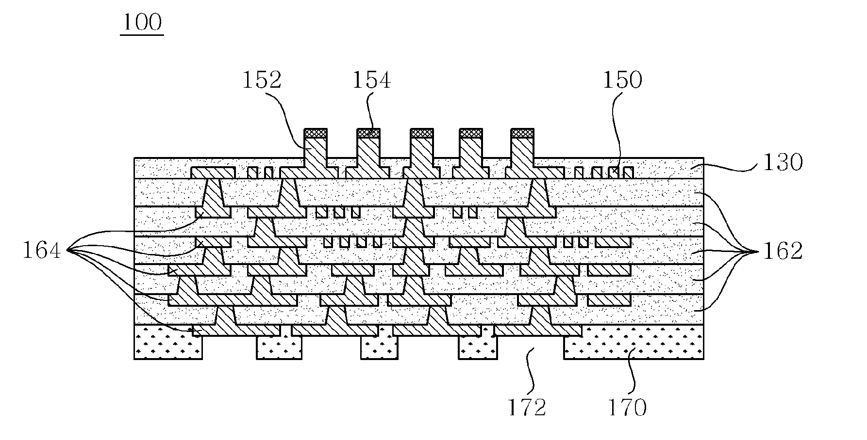
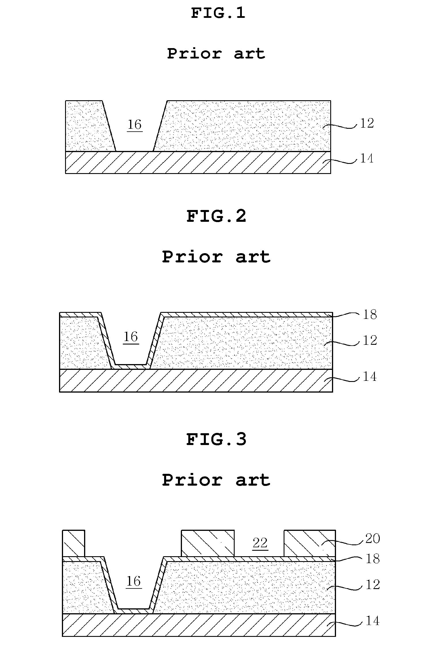
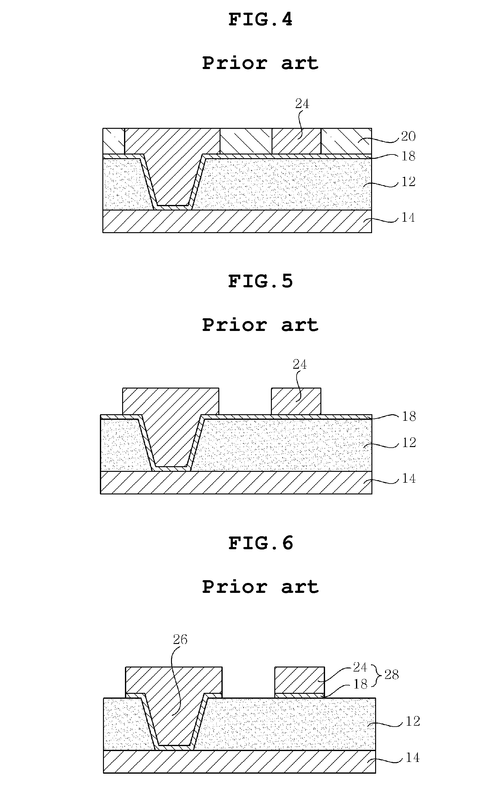
[0042]Hereinafter, a detailed description will be given of embodiments of the present invention with reference to the accompanying drawings. Throughout the drawings, the same reference numerals refer to the same or similar elements, and redundant descriptions are omitted. In the description, in the case where known techniques pertaining to the present invention are regarded as unnecessary because they make the characteristics of the invention unclear and also for the sake of description, the detailed descriptions thereof may be omitted.

[0043]Furthermore, the terms and words used in the present specification and claims should not be interpreted as being limited to typical meanings or dictionary definitions, but should be interpreted as having meanings and concepts relevant to the technical scope of the present invention based on the rule according to which an inventor can appropriately define the concept implied by the term to best describe the method he or she knows for carrying out...


PUM

PropertyMeasurementUnit
thicknessaaaaaaaaaa
thicknessaaaaaaaaaa
signal transmission speedaaaaaaaaaa

Abstract

Disclosed is a printed circuit board, which includes an insulating member having a circuit pattern embedded in one surface thereof, a bump pad formed in the insulating member so as to be connected to the circuit pattern and protruding from an outer surface of the insulating member, a build-up layer formed on one surface of the insulating member and including a build-up insulating layer and a circuit layer formed in the build-up insulating layer and having a via connected to the circuit pattern, and a solder resist layer formed on the build-up layer. A method of fabricating the printed circuit board is also provided. The printed circuit board is fabricated using a build-up process and the outermost circuit layer thereof is formed to have an embedded structure using an imprinting process, thus minimizing the separation of the circuit layer and reducing the lead time and the fabrication cost.

Description

CROSS REFERENCE TO RELATED APPLICATION[0001]This application claims the benefit of Korean Patent Application No. 10-2009-0070637, filed Jul. 31, 2009, entitled “A printed circuit board and a fabricating method the same”, which is hereby incorporated by reference in its entirety into this application.BACKGROUND OF THE INVENTION[0002]1. Technical Field[0003]The present invention relates to a printed circuit board (PCB) and a method of fabricating the same.[0004]2. Description of the Related Art[0005]Recently, in order to cope with an increase both in signal transmission speed and density of a semiconductor chip, the demand for techniques for directly mounting a semiconductor chip on a PCB is increasing. Thus, the development of a PCB having high density and high reliability capable of coping with the increase in the density of the semiconductor chip is required.[0006]The requirements for the PCB having high density and high reliability are closely related to the specs of the semicondu...

Claims


Application Information

Patent Timeline
Patent Type & Authority Applications(United States)
IPC IPC(8): H05K1/11H05K3/10
CPCH05K3/4007H05K3/0097H05K2203/1536Y10T29/49155H05K3/4682H05K3/107H05K2201/0367H05K2201/0352Y10T29/49204H05K1/114H05K3/18H05K3/40H05K3/46
Inventor KO, YOUNG GWAN
Owner SAMSUNG ELECTRO MECHANICS CO LTD
Why Eureka
Try Eureka