Creation of thin group ii-vi monocrystalline layers by ion cutting techniques

a monocrystalline layer and ion cutting technology, applied in the direction of basic electric elements, electrical apparatus, semiconductor devices, etc., can solve the problems of high cost of single-crystal cdte, and mechanically not very robus

Inactive Publication Date: 2011-02-03
EPIR TECH INC
View PDF7 Cites 23 Cited by
  • Summary
  • Abstract
  • Description
  • Claims
  • Application Information

AI Technical Summary

Problems solved by technology

On the other hand, single-crystal CdTe, like other single-crystal Group II-VI semiconductors, is very expensive and mechanically not very robust.

Method used


Image

  • Creation of thin group ii-vi monocrystalline layers by ion cutting techniques
  • Creation of thin group ii-vi monocrystalline layers by ion cutting techniques
  • Creation of thin group ii-vi monocrystalline layers by ion cutting techniques

Examples


Embodiment Construction

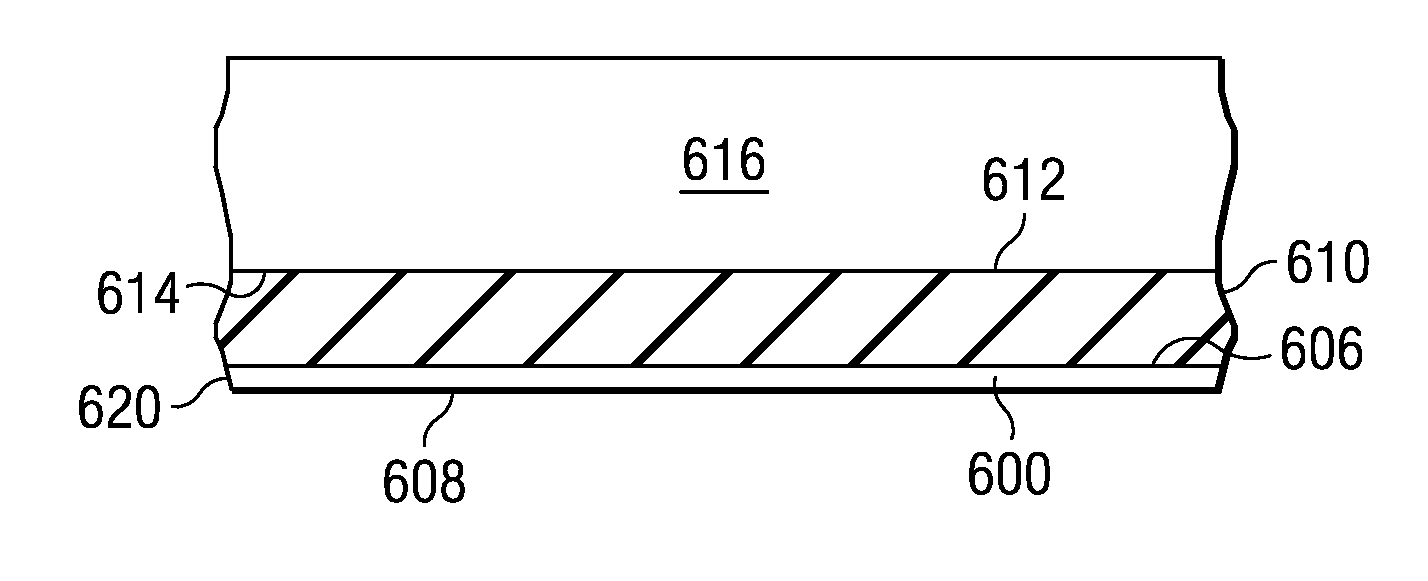
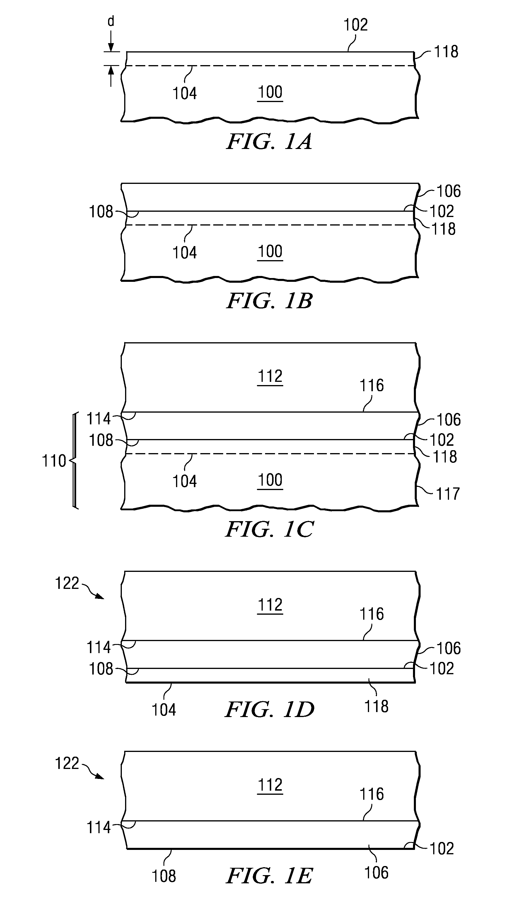
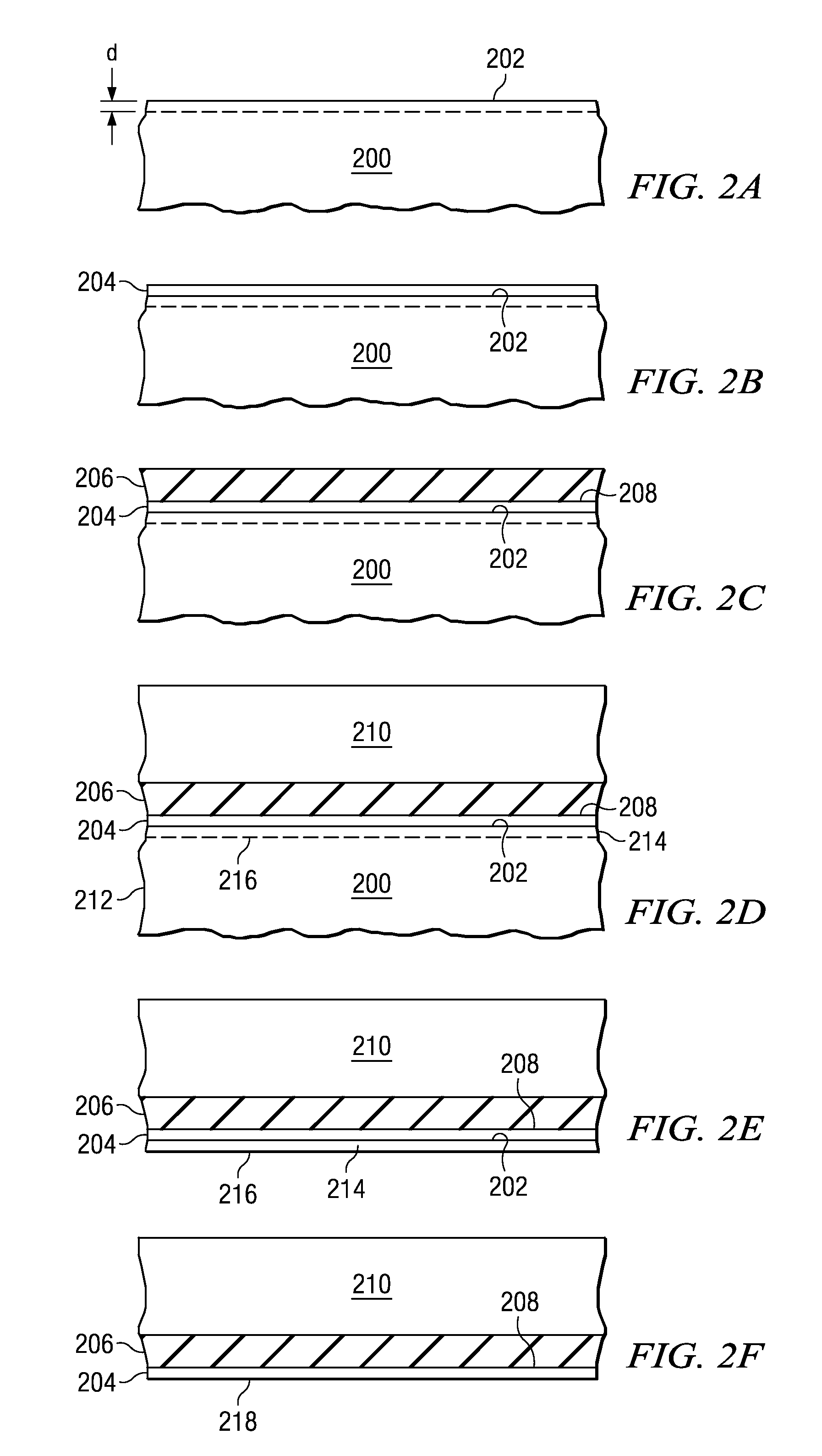
[0026]Referring first to FIGS. 1A-1E, successive steps in a first ion cut process according to the invention are illustrated. A first, preselected substrate 100 is provided, which can be made of a relatively inexpensive material such as elemental silicon. Alternatively the first substrate can be another Group IV monocrystalline substrate, such as an alloy of Silicon and Germanium, or a silicon on insulator (SOI) structure in which a silicon portion is uppermost as appears in these FIGUREs. The substrate 100 can also consist or comprise a Group III-V semiconductor or a Group II-VI semiconductor. The substrate 100 should be thick enough to be mechanically robust and successfully resist degrading forces placed upon it during the rest of the process steps described herein, including mechanical, chemical and thermal treatments encountered in semiconductor processing. An upper surface 102 of the substrate 100 may be chosen to be in a plane which will present a crystalline structure which ...


PUM


Abstract

Expungement ions, preferably including hydrogen ions, are implanted into a face of a first, preferably silicon, substrate such that there will be a maximum concentration of the expungement ions at a predetermined depth from the face. Subsequently a monocrystalline Group II-VI semiconductor layer, or two or more such layers, is / are grown on the face, as by means of molecular beam epitaxy. After this a second, preselected substrate is attached to an upper face of the Group II-VI layer(s). Next, the implanted expungement ions are used to expunge most of the first substrate from a remnant thereof, from the grown II-VI layer, and from the second substrate. In another embodiment, a group II-VI layer is grown on a first substrate silicon and an ionic implantation is conducted such that a maximum concentration of expungement ions occurs either in the silicon substrate at a predetermined depth from its interface with the II-VI layer or in the first Group II-VI semiconductor layer at a predetermined depth from the top face of the Group II-VI semiconductor layer. Thereafter all of the first substrate is expunged from the rest of the workpiece. Thin monocrystalline Group II-VI semiconductor structures may thus be mounted to substrates of the fabricator's choice; these substrates may be semiconductors, integrated circuits, MEMS structures, polymeric, metal or glass, may be flexible and may be curved.

Description

BACKGROUND OF THE INVENTION[0001]Single-crystal CdTe is a very useful semiconductor material for a variety of uses for optoelectronic devices such as solar cells, infrared detectors and cameras. On the other hand, single-crystal CdTe, like other single-crystal Group II-VI semiconductors, is very expensive and mechanically not very robust. For this reason the assignee of this invention has developed methods and structures for producing thin single-crystal CdTe on silicon. [1,2] This helps reduce cost, as a silicon substrate is much less expensive than other substrates that have been used as CdTe hosts in the art. It has now been shown that II-VI semiconductor homojunctions grown on Si make extremely efficient relatively inexpensive multijunction solar cells. [3] The present invention discloses ways in which silicon can continue to be used as a host for growing a CdTe layer, but in which the silicon substrate can either be greatly reduced or entirely omitted in the final semiconductor...

Claims


Application Information

Patent Timeline
Patent Type & Authority Applications(United States)
IPC IPC(8): H01L29/22H01L21/04
CPCH01L21/76254H01L31/1828Y02E10/543H01L31/1836H01L31/1892H01L31/1832
Inventor BOWER, ROBERT W.SIVANANTHAN, SIVALINGAMGARLAND, JAMES W.
Owner EPIR TECH INC
Why Eureka
Try Eureka