Optical display device manufacturing system and method for manufacturing optical display device

a manufacturing system and optical display technology, applied in non-linear optics, instruments, optics, etc., can solve problems such as increasing manufacturing costs, and achieve the effect of improving the contrast of optical display devices and simplifying the constitution

Inactive Publication Date: 2011-02-03
NITTO DENKO CORP
View PDF9 Cites 21 Cited by
  • Summary
  • Abstract
  • Description
  • Claims
  • Application Information

AI Technical Summary

Benefits of technology

[0031]In accordance with this constitution, the first optical film which is fed from the first material roll and cut, and the second optical film which is fed from the second material roll and cut are bonded respectively to both the surfaces of the liquid crystal cell in such a manner that the absorption axes thereof are orthogonal to each other. Accordingly, since it is possible to set the first optical film and the second optical film, which are bonded respectively to both the surfaces of the liquid crystal cell, to the crossed nicols relation, without setting the mechanism for rotating the liquid crystal cell or the like, it is possible to bond the optical films to both the surfaces of the liquid crystal cell in good condition with a simpler constitution.
[0032]Particularly, since the first optical film is wound in such a manner that the absorption axis extends in the orthogonal direction to the width direction, and the second optical film is wound in such a manner that the absorption axis extends in the width direction, it is easy to align the absorption axis of each of the optical films with the long side or short side of the liquid crystal cell. Accordingly, since there is a low possibility that the absorption axis is deviated at a time of bonding the optical film to the liquid crystal cell, and the contrast abnormality of the optical display device caused by the deviation of the absorption axis is hardly generated, it is possible to bond the optical films to both the surfaces of the liquid crystal cell in good condition. Further, it is possible to effectively improve the contrast of the optical display device.
[0034]In accordance with this constitution, it is possible to bond the first optical film and the second optical film to both the surfaces of the liquid crystal cell in parallel at least at a certain period. Accordingly, since it is possible to simultaneously or continuously bond the first optical film and the second optical film in a state in which the liquid crystal cell is positioned, it is not necessary to position the liquid crystal cell at a time of bonding respectively, such as the case of independently bonding the first optical film and the second optical film. Accordingly, it is possible to cut down a positioning device, and it is possible to bond the optical films to both the surfaces of the liquid crystal cell in good condition with a simpler constitution.
[0036]In accordance with this constitution, it is possible to relatively position the first optical film and the second optical film, and it is possible to precisely bond them to the liquid crystal cell in the crossed nicols relation. Accordingly, it is possible to bond the optical films to both the surfaces of the liquid crystal cell in good condition.

Problems solved by technology

However, there are a problem of a manufacturing cost increase caused by multiple steps, a problem of the scratch, the dust, the dirt and the like generated by the multiple steps and the transport, a necessity of the inspection step caused thereby, and a problem that it is necessary to store and manage many kinds of optical films as a stock.

Method used


Image

  • Optical display device manufacturing system and method for manufacturing optical display device
  • Optical display device manufacturing system and method for manufacturing optical display device
  • Optical display device manufacturing system and method for manufacturing optical display device

Examples


first embodiment

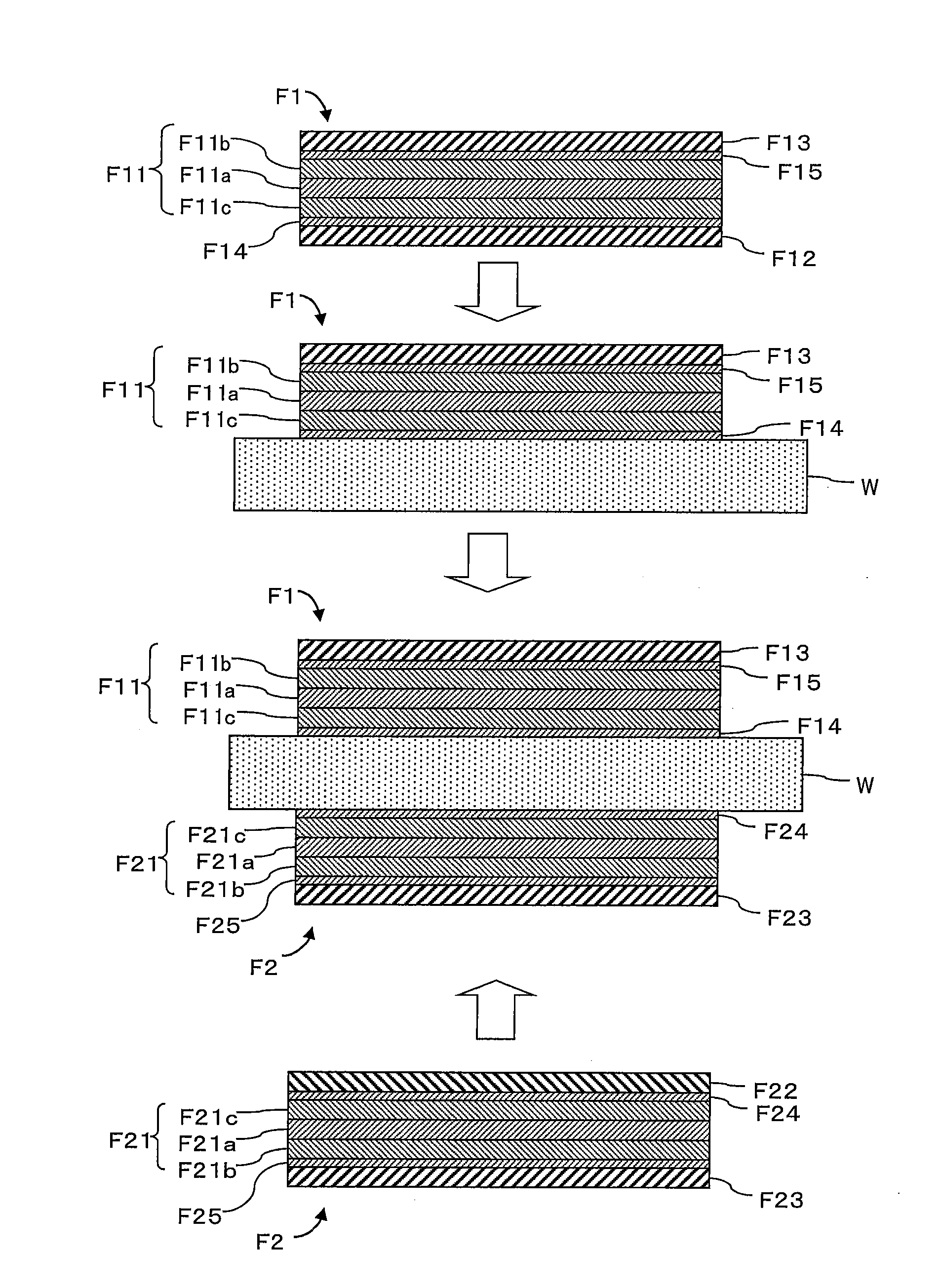
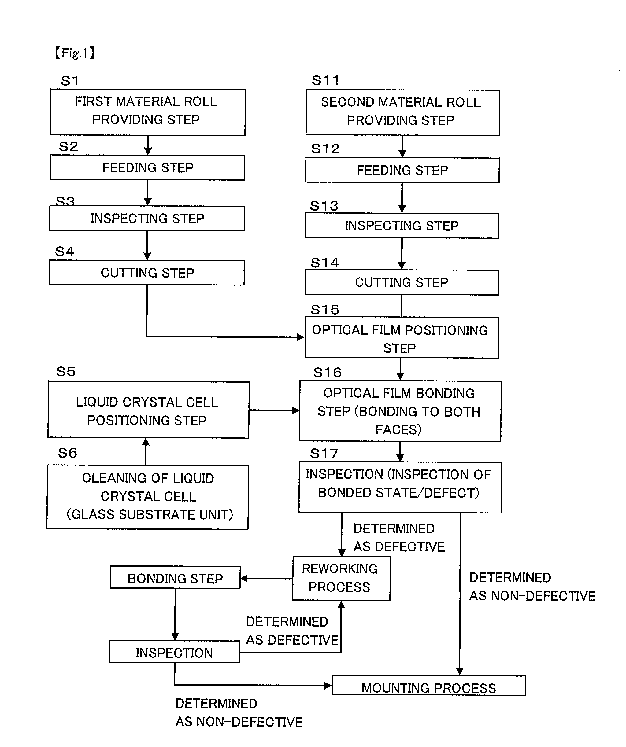
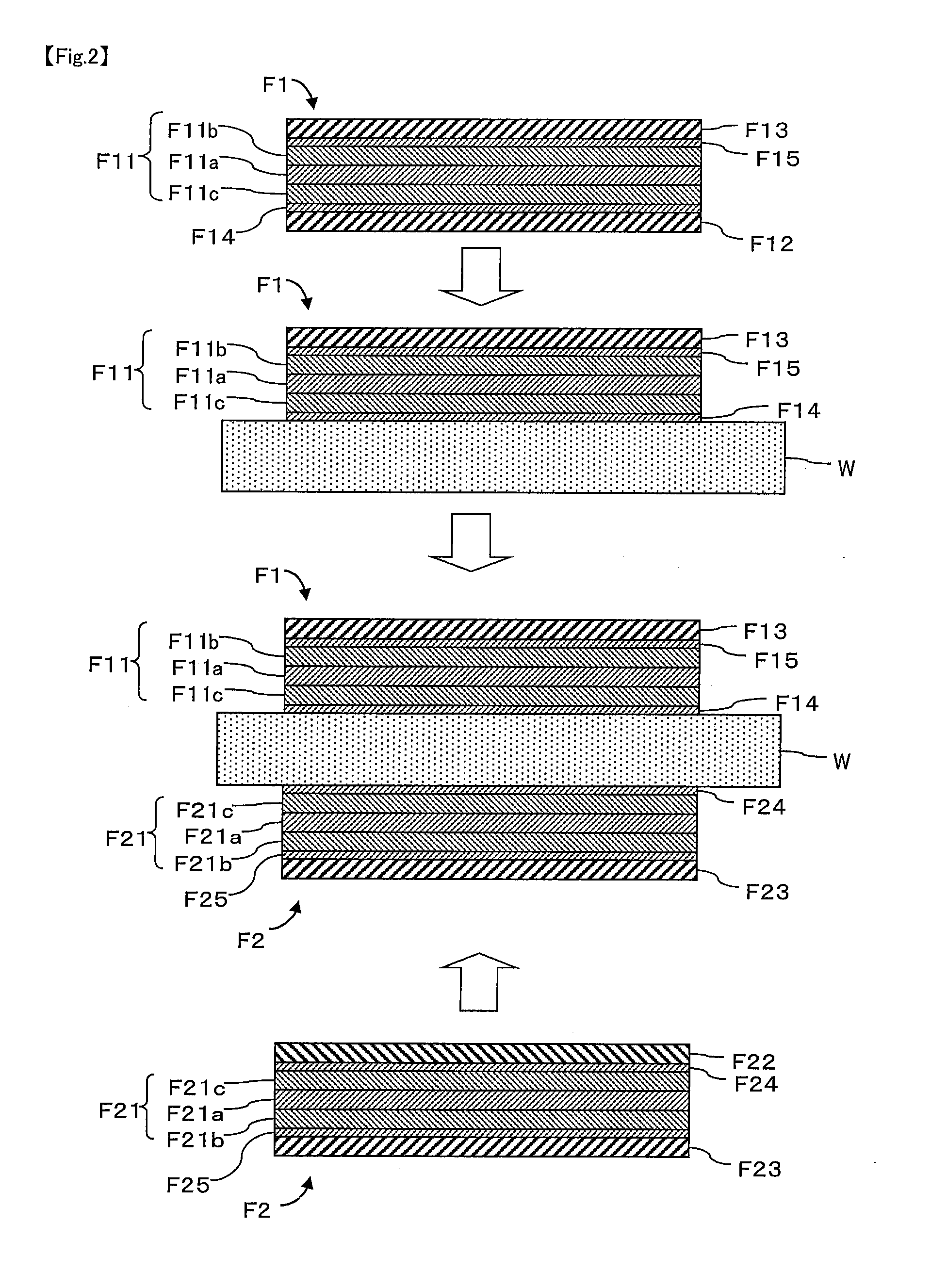
[0077]A description will be given below for a first embodiment in accordance with the present invention. FIG. 1 shows a flow chart of a manufacturing method of an optical display device in accordance with the first embodiment. A construction which is not provided with first and second defect inspection apparatuses, can be exemplified as the other embodiment of the manufacturing system in accordance with the first embodiment.

[0078](Liquid Crystal Cell)

[0079]First, for example, a glass substrate unit, an organic electroluminescent (EL) light-emitting unit and the like can be listed up, as a liquid crystal cell used in the present invention. The liquid crystal cell is formed, for example, as a rectangular shape.

[0080](Optical Film)

[0081]An optical film to be bonded to the liquid crystal cell is a film including a polarizer (a polarizer film), or may be a laminated film in which another film such as a retardation film, a brightness enhancement film or the like is combined with it. There...

reference example 1

[0155]Preparation of polarization plate A: A polyvinyl alcohol film having a polymerization degree of 2700 and a thickness of 75 μm was fed from a material roll, stretched 1.2 folds in a feeding direction while being swollen for one minute in a water bath at 30° C., thereafter dipped in an aqueous solution having a potassium iodide concentration of 0.03% and an iodine concentration of 0.3% at 30° C. for 60 minutes so as to be dyed, and stretched 3 folds totally in a film feeding direction. Next, it was stretched totally 6 folds while being dipped in an aqueous solution having a boric acid concentration of 4% and a potassium iodide concentration of 5% at 60° C. for 30 seconds. Finally, it was cleaned by being dipped in an aqueous solution having a potassium iodide concentration of 2% at 30° C. for several seconds, and a polarizer was obtained by drying the obtained stretched film at 70° C. for 2 minutes. A polarizing plate A having a polarization axis (an absorption axis) in an ortho...

reference example 2

[0158]Preparation of polarizing plate C: A base material film “TD80UL manufactured by Fujifilm Corporation” was fed from a material roll, and a solution obtained by preparing a polyimide synthesized from 2,2′-bis(3,4-dicarboxyphenyl)hexafluoropropane≅6FDA and 2,2′-bis(trifluoromethyl)-4,4′-diaminobiphenyl≅PFMB≅TFMB at 15 wt % by using cyclohexanone as a solvent was applied at a thickness of 20 μm. A base material film with thin film of about 3 μm in thickness was obtained thereafter applying a drying process at 100° C. for 10 minutes. The retardation of the obtained base material film with thin film was measured by using “KOBRA (registered mark) 21ADH manufactured by Oji Scientific Instruments), the front retardation was 1.2 nm, and the retardation in a thickness direction was 188 nm. A base material film B with retardation was made by fixed-end uniaxial stretching (tenter stretching) of the base material film with thin film at 1.19 folds in the width direction at 160° C. The retard...


PUM

PropertyMeasurementUnit
thicknessaaaaaaaaaa
transmittanceaaaaaaaaaa

Abstract

Provided are an optical display device manufacturing system and a method for manufacturing an optical display device which can bond optical films to both surfaces of a liquid crystal cell in good condition with a simpler constitution. A first optical film F11 is fed in an orthogonal direction with respect to the width direction from a first material roll R1 formed by winding the first optical film F11 in such a manner that an absorption axis B1 extends in the orthogonal direction, and then the first optical film F11 is cut and bonded to one surface of a liquid crystal cell. A second optical film F21 is fed in an orthogonal direction with respect to the width direction from a second material roll R2 formed by winding the second optical film F21 in such a manner that an absorption axis B2 extends in the width direction, and then the second optical film F21 is cut and bonded to the other surface of the liquid crystal cell. Accordingly, it is possible to bond the first optical film F11 and the second optical film F21 in the crossed nicols relation, without the provision of the mechanism for rotating the liquid crystal cell W or the like.

Description

TECHNICAL FIELD[0001]The present invention relates to an optical display device manufacturing system and a method for manufacturing an optical display device for manufacturing an optical display device by feeding an optical film from a material roll, which is formed by winding the optical film, and bonding the film to a liquid crystal cell.BACKGROUND ART[0002]A manufacturing method of an optical display device mounted to a conventional liquid crystal display device is conceptually shown in FIG. 6. First, in an optical filmmaker, a step produces a long (web-like) optical film as a material roll (#1). The concrete manufacturing step is a known manufacturing step, and a description thereof will not be given. As the long (web-like) optical film as a material roll, for example, there are a polarizing plate material, a retardation plate material, a laminated film material of the polarizing plate and the retardation plate, and the like which are used in a liquid crystal display device. Nex...

Claims


Application Information

Patent Timeline
Patent Type & Authority Applications(United States)
IPC IPC(8): G02F1/1335G02F1/13
CPCG02F1/1303G02F1/1335G02F1/1333
Inventor KOSHIO, SATORUNAKAZONO, TAKUYAKITADA, KAZUOYURA, TOMOKAZUTAKEDA, KENTAROU
Owner NITTO DENKO CORP
Why Eureka
Try Eureka