Method of driving storage device

a storage device and drive technology, applied in the direction of digital storage, semiconductor devices, instruments, etc., can solve the problems of dielectric breakdown, destructing the resistance element itself, and difficulty in stably holding written data, so as to prevent the diffusion loss of the conductive path, and variable

Active Publication Date: 2011-02-03
SONY SEMICON SOLUTIONS CORP
View PDF4 Cites 3 Cited by
  • Summary
  • Abstract
  • Description
  • Claims
  • Application Information

AI Technical Summary

Benefits of technology

[0010]In view of the foregoing, it is an object of the present invention to provide a method of driving a storage device capable of improving reliability of data write in the storage device including a variable resistance element.
[0012]In the method of driving a storage device of the present invention, when the voltages are applied between the pair of electrodes in the variable resistance element, a conductive path is formed between the pair of electrodes, and a current flows. Thereby, the variable resistance element is changed from the high resistance state to the low resistance state, and data is written. Here, at the time of such data write operation (when changing from the high resistance state to the low resistance state), the plurality of pulse voltages having shapes different from each other are applied between the pair of electrodes, and thus it is possible to prevent diffusion loss of the conductive path caused by self-heat generation of the variable resistance element. Also, the variable resistance element may be prevented from being destructed when the write operation is sufficiently performed.
[0013]In the method of driving a storage device of the present invention, two pulse voltages having shapes different from each other may be applied between the pair of electrodes, when the variable resistance element is changed from the high resistance state to the low resistance state. In this case, in the two pulse voltages, a voltage value of a second pulse voltage may be set to be lower than a voltage value of a first pulse voltage. In the case of such a configuration, after the data write operation is performed with the first write pulse voltage, the self-heat generation of the variable resistance element is suppressed with the second pulse voltage having the lower voltage value, and it is possible to prevent the diffusion loss of the conductive path caused by a non-bias state between the pair of electrodes. Therefore, the resistance value of the variable resistance element in the low resistance state after the write operation is stabilized, and written data is stably held.
[0014]Also, in the case where the two pulse voltages having shapes different from each other are applied as described above, in the two pulse voltages, the voltage value of the second pulse voltage may be set to be higher than the voltage value of the first pulse voltage. In the case of such a configuration, after the variable resistance element becomes a soft-breakdown state with the first pulse voltage having the lower voltage value, the conductive path in a sufficient amount is formed with the second pulse voltage having the higher voltage value. Thus, the write operation is sufficiently performed. Accordingly, generation of error at the time of the write operation (write error) is suppressed while destruction and deterioration of the variable resistance element are prevented, and it is possible to stably perform the write operation.
[0015]According to the method of driving the storage device of the present invention, at the time of the data write operation (when changing from the high resistance state to the low resistance state), the plurality of pulse voltages having shapes different from each other are applied between the pair of electrodes, and thus it is possible to prevent the diffusion loss of the conductive path caused by the self-heat generation of the variable resistance element, and prevent the variable resistance element from being destructed when the write operation is sufficiently performed. Therefore, it is possible to stabilize the data write operation and data hold operation, and it is possible to improve reliability of the data write operation.

Problems solved by technology

And, when the variation of the resistance is large in this manner, it is difficult to stably hold the written data.
However, when a voltage unnecessarily high is applied to the variable resistance element, or a high current is flown too much, there is a case where the insulating film causes dielectric breakdown, and the variable resistance element itself is destructed.
In this manner, in the existing storage device, it is difficult to stably write and hold the data, and thus it is difficult to enhance reliability.

Method used


Image

  • Method of driving storage device
  • Method of driving storage device
  • Method of driving storage device

Examples


first embodiment

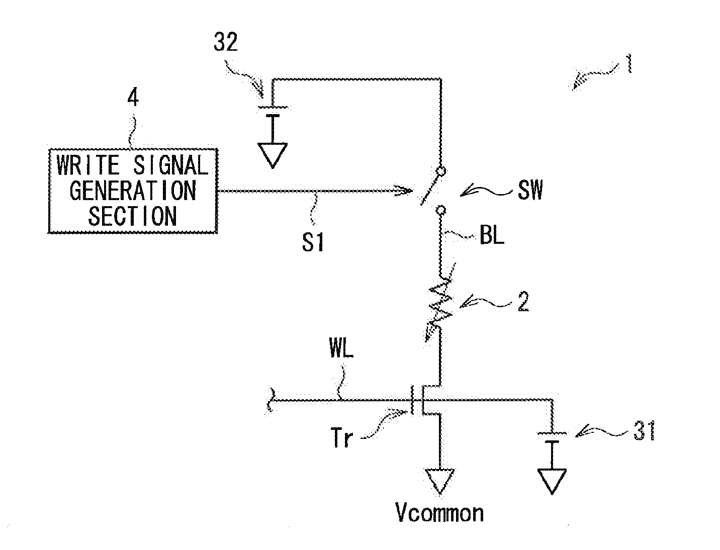
[0025]FIG. 1 illustrates a circuit configuration example of a memory cell 1 in a storage device to which a method of driving a storage device according to a first embodiment of the present invention is applied. This memory cell 1 includes a variable resistance element 2, a selection transistor Tr, a gate voltage power supply 31, a switch SW, a write voltage power supply 32, and an erase voltage power supply (not illustrated in the figure). In addition, a plurality of the memory cells 1 having such a configuration are arranged, for example, in a matrix form, and thereby the storage device (memory) is configured.

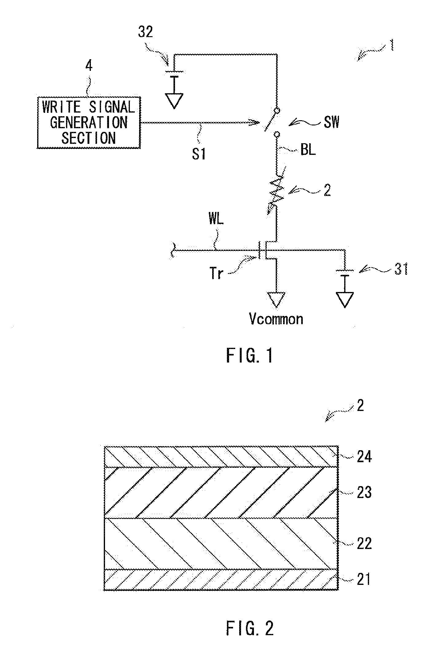
[0026]The variable resistance element 2 includes a pair of electrodes which will be described later, and is configured so that the resistance value is reversibly changed by applying voltages of different polarities (a write voltage and an erase voltage which will be described later) between the pair of electrodes. In addition, a detailed configuration of this variable resistan...

second embodiment

[0048]Next, a second embodiment of the present invention will be described. In addition, same reference numerals are used to indicate components identical to those in the first embodiment, and thereby the description is appropriately omitted.

[0049]FIG. 8 illustrates an example of the data write method according to this embodiment, and specifically illustrates the timing waveform at the time of the data write operation. In addition, the storage device to which the data write method according to this embodiment is applied is the same as that described in the first embodiment, and thereby the description is omitted.

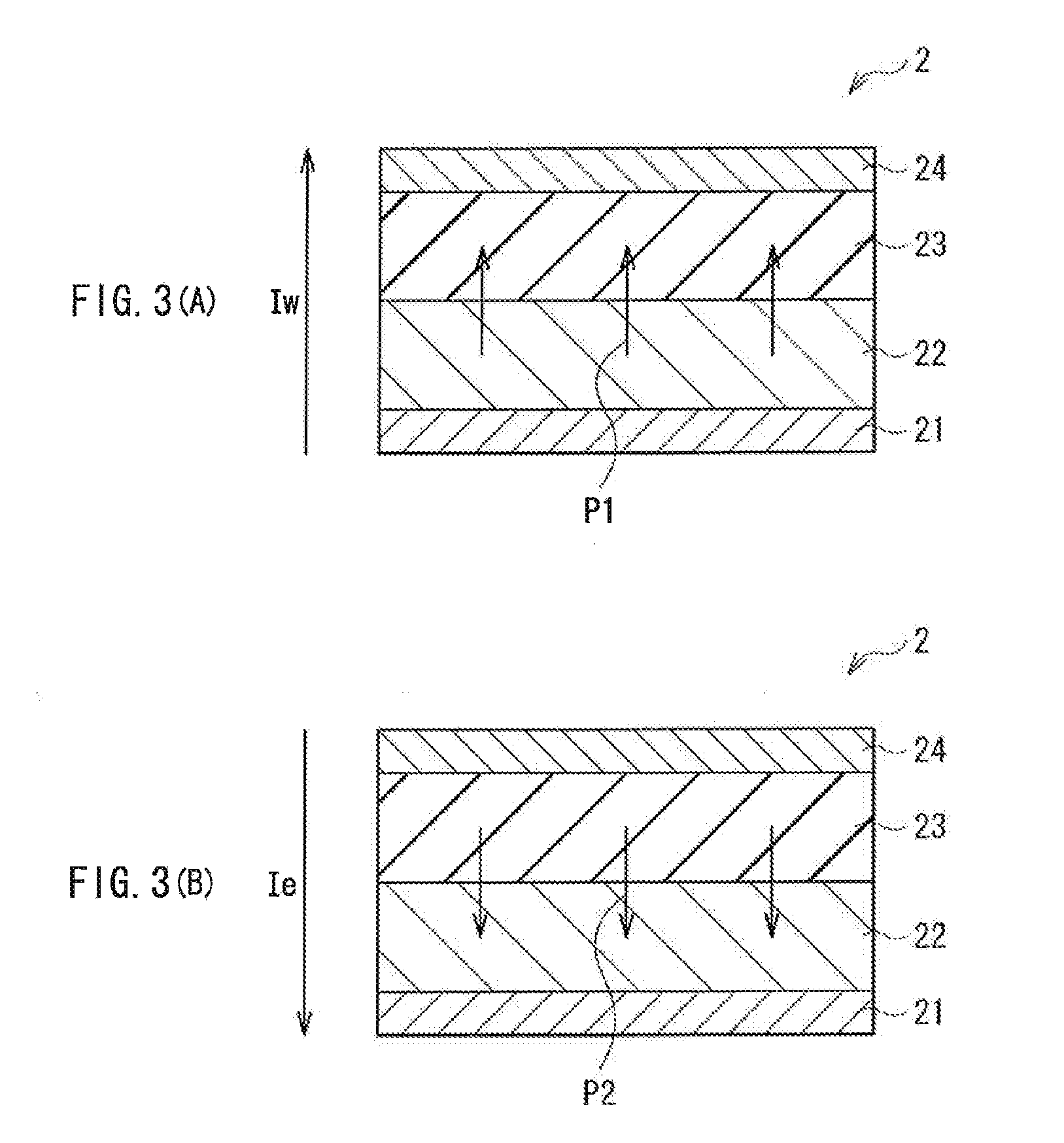
[0050]Here, first, before describing the data write method of this embodiment, the data write operation will be studied in detail. It is considered that this data write operation is configured with two steps. Fist, in the first step, the write voltage is applied between the electrodes 21 and 24 in the high resistance state of insulation properties, and soft-breakdown is gene...


PUM


Abstract

Provided is a method of driving a storage device capable of improving reliability of data write in the storage device including a variable resistance element. At the time of data write operation, a plurality of write pulses having shapes different from each other are applied between electrodes 21 and 24 in a variable resistance element 2. Diffusion loss of a conductive path caused by self-heat generation (generation of Joule heat) of the variable resistance element 2 may be prevented, and thus data hold operation after write is stabilized. Also, the variable resistance element 2 may be prevented from being destructed when the write operation is sufficiently performed, and thus the data write operation is stabilized.

Description

TECHNICAL FIELD[0001]The present invention relates to a method of driving a storage device when a variable resistance element is changed from a high resistance state to a low resistance state (write operation) in the storage device in which a memory cell is composed of a nonvolatile variable resistance element.BACKGROUND ART[0002]An existing storage device, in particular, a storage device using a flash memory has been actively used in recent years, since the electric power for holding storage data is unnecessary. In particular, in a portable terminal device including a cell-phone unit, a flash memory has been widely used as a memory. However, in a storage device using such a flash memory, there is an issue that the data write speed is slow (for example, refer to Non-patent Document 1).[0003]Thus, the applicant has proposed a storage device using a nonvolatile variable resistance element which may have characteristics superior to those of the above-described flash memory (for example...

Claims


Application Information

Patent Timeline
Patent Type & Authority Applications(United States)
IPC IPC(8): G11C11/00
CPCG11C13/00G11C13/0061G11C13/0069G11C2013/0092G11C2213/56G11C2013/0073H01L45/085H01L45/1266H01L45/146G11C2013/0071H01L27/101H10N70/245H10N70/8416H10N70/8833
Inventor SHIIMOTO, TSUNENORIOKAZAKI, NOBUMICHITSUSHIMA, TOMOHITO
Owner SONY SEMICON SOLUTIONS CORP
Why Eureka
Try Eureka