Microelectronic device and fabricating method thereof and MEMS package structure and fabricating method thereof

a microelectronic device and package structure technology, applied in the field of microelectronic devices, mems package structure and fabricating methods thereof, can solve the problems of failure to achieve commercialization, complicated and difficult process and low production cost of microelectronic devices, so as to improve the performance of microelectronic devices, simplify the packaging procedure, and reduce the production cost of conventional microelectronic devices

Active Publication Date: 2011-02-17
PIXART IMAGING INC
View PDF21 Cites 29 Cited by
  • Summary
  • Abstract
  • Description
  • Claims
  • Application Information

AI Technical Summary

Benefits of technology

[0019]In the fabricating method of the microelectronic device of the present invention, the CMOS circuit and the MEMS element may be integrated into a wafer by CMOS process. Furthermore, the MEMS structure can be packaged by CMOS process so that the packaging procedure of the microelectronic device can be simplified, and thus the production cost of the microelectronic device can be reduced. In addition, the microelectronic device and the fabricating method thereof can solve the stiction problem that is associated with the MEMS element due to phosphorus ions. Therefore, the performance of the microelectronic device can be improved.

Problems solved by technology

However, the fabrication procedure of the conventional microelectronic device is complicated and difficultly, so the microelectronic device tends to have a relatively high production cost and fail to achieve commercialization.

Method used


Image

  • Microelectronic device and fabricating method thereof and MEMS package structure and fabricating method thereof
  • Microelectronic device and fabricating method thereof and MEMS package structure and fabricating method thereof
  • Microelectronic device and fabricating method thereof and MEMS package structure and fabricating method thereof

Examples


Embodiment Construction

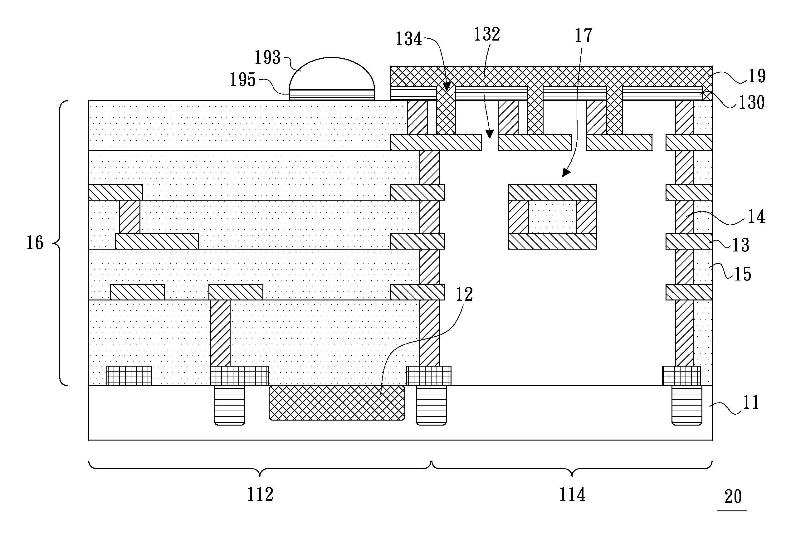
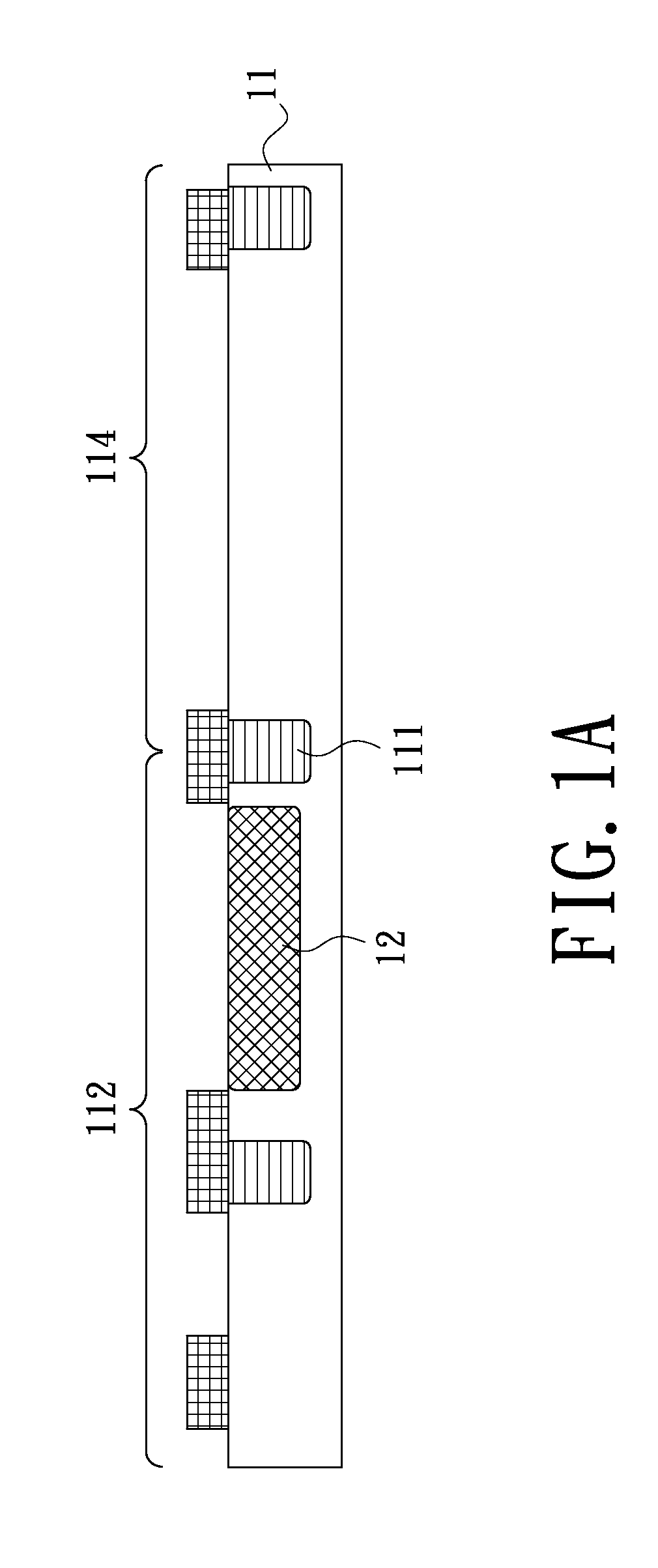
[0026]FIGS 1A to 1E are schematic views of a microelectronic device during a fabricating process thereof according to an embodiment of the present invention. Referring to FIG. 1A, firstly, a substrate 11 having a CMOS circuit region 112 and a MEMS region 114 is provided. The substrate 11 can be a silicon substrate or a substrate of silicon on insulator (SOI). Secondly, a semi-conductor element 12 is formed in the CMOS circuit region 112 of the substrate 11. In alternative embodiment, a plurality of semi-conductor elements 12 can be formed in the CMOS circuit region 112 and spaced by shallow trench insulation (STI) 111 therebetween.

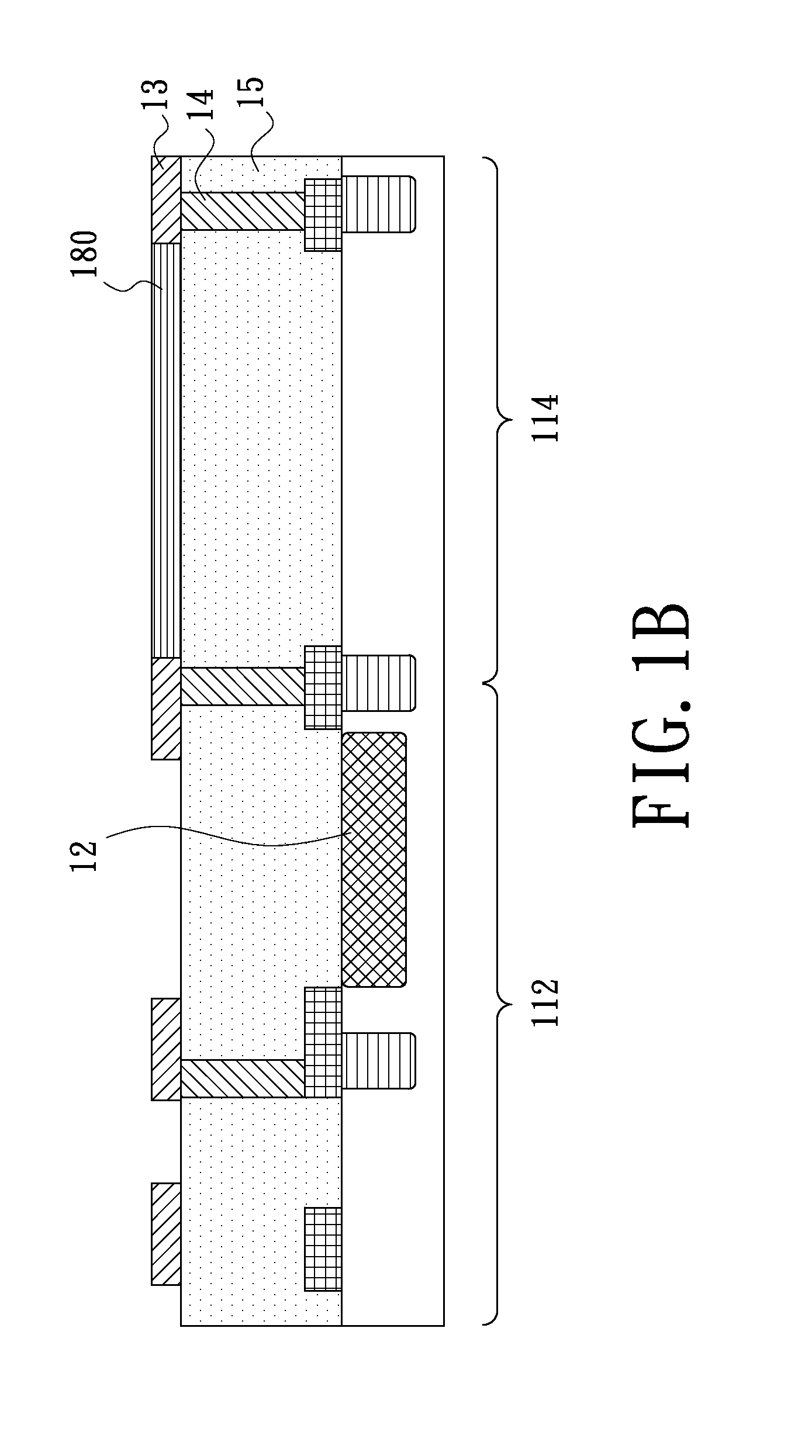
[0027]Referring to FIG. 1B, at least a metallic layer 13 and at least an oxide layer 15 are formed on the substrate 11, and a plurality of contact plugs 14 are formed in the oxide layer 15. Next, a protective layer 180 is formed on a portion of the oxide layer 15 within the MEMS region 114. In this embodiment, material of the protective layer 180 can be am...


PUM


Abstract

A fabricating method of a microelectronic device including the following steps is provided. First, a substrate is provided. Second, a semi-conductor element is formed in a CMOS circuit region of the substrate. Next, a plurality of metallic layer, a plurality of contact plugs and a plurality of oxide layer are formed on the substrate. The metallic layers and the oxide layers are interlaced with each other and the contact plugs are formed in the oxide layers and connected with the metallic layers correspondingly so as to form a micro electromechanical system (MEMS) structure within a MEMS region and an interconnecting structure within the CMOS circuit region. Then, a first protective layer is formed on at least one of the oxide layers and a second protective layer is formed on the interconnecting structure. Predetermined portions of the oxide layers located within the MEMS region are removed and thereby the MEMS structure is partially suspended above the substrate. The present invention also provides a microelectronic device, a MEMS package structure and a fabricating method thereof

Description

[0001]This application claims priority to a Taiwan application No. 098126961 filed Aug. 11, 2009.BACKGROUND[0002]1. Technical Field[0003]The present invention relates to a microelectronic device, a MEMS package structure and fabricating methods thereof, and more particularly to a microelectronic device, a MEMS package structure and fabricating methods thereof with low production cost.[0004]2. Description of the Related Art[0005]Micro Electromechanical System (MEMS) technique has established a whole new technical field and industry. The MEMS technique has been widely used in a variety of microelectronic devices that have electronic and mechanical properties, for example, pressure sensors, accelerators and micro-microphones.[0006]For a conventional microelectronic device including MEMS elements, the interior semi-conductor circuits are generally fabricated by CMOS process, and the MEMS elements are fabricated by external micro-machining process. However, the fabrication procedure of t...

Claims


Application Information

Patent Timeline
Patent Type & Authority Applications(United States)
IPC IPC(8): H01L23/52H01L21/768H01L31/18H01L21/60H01L23/48
CPCB81C1/00246B81C1/00333B81C2203/0714H01L21/768B81C2203/0145H01L27/14632B81B3/0018B81C1/00015H01L27/1443
Inventor HSU, HSIN-HUILEE, SHENG-TAWANG, CHUAN-WEI
Owner PIXART IMAGING INC
Why Eureka
Try Eureka