Three Dimensionally Structured Thin Film Photovoltaic Devices with Self-Aligned Back Contacts

a technology of back contacts and thin films, applied in the field of photovoltaic devices, can solve the problems of affecting the performance of photovoltaic devices, reducing the efficiency of light conversion, and challenging the ability to ensure uninterrupted connectivity

Inactive Publication Date: 2011-02-24
GOVERNMENT OF THE UNITED STATES OF AMERICA AS REPRESENTED BY THE SEC OF COMMERCE THE NAT INST OF STANDARDS & TEHCNOLOGY
View PDF4 Cites 12 Cited by
  • Summary
  • Abstract
  • Description
  • Claims
  • Application Information

AI Technical Summary

Benefits of technology

[0021]In a second step, the method for forming a multijunction device comprises electrodepositing one or more thin films of one or more of a second semiconducting material onto at least said first interdigitated electrode but without impinging upon said second interdigitated electrode, the second semiconducting material being the other type of an n-type or p-type material. In a third step, the method comprises electrodepositing one or more thin films of one or more of a third semiconducting material onto either the first or second interdigitated electrode without impinging on the other of the first or second interdigitated electrode, the third semiconducting material being either the same type as the first semiconducting material if electrodeposited on the first interdigitated electrode, or the same type as the second semiconducting material if electrodeposited on the second interdigitated electrode, wherein the third semiconducting material is either an n-type or p-type material.
[0022]In a fourth step, the method for forming a multijunction device comprises depositing one or more thin films of one or more of a fourth semiconducting material onto one or more of the at least two interdigitated electrodes, wherein the depositing occurs at least until the thin films on the first interdigitated electrode and the second interdigitated electrodes impinge upon each other, wherein the fourth semiconducting material is the other of said either an n-type or p-type material electrodeposited in the third step. After fabrication of the multijunction photovoltaic device, at least two of said at least two interdigitated electrodes serve as the back contacts for carrier extraction when the device is in use.
[0023]In accordance with yet another embodiment of the present disclosure, a three dimensionally structured thin film photovoltaic device is provided with self-aligned back contacts that are formed by electrodeposition on interdigitated electrodes used in the device's manufacture. The device comprises an insulating substrate, and at least two interdigitated electrodes on the insulating substrate, the at least two interdigitated electrodes including a plurality of interdigitated wires having pitches of less than ten micrometers, wherein the at least two interdigitated electrodes include a first interdigitated electrode and a second interdigitated electrode. The device also comprises one or more electrodeposited thin film layers of one or more of a first semiconducting material on the first interdigitated electrode, wherein the first semiconducting material is either an n-type or p-type material. The device further comprises one or more deposited thin film layers of one or more of a second semiconducting material on the second interdigitated electrode, wherein the deposits on the first interdigitated electrode and the second

Problems solved by technology

On the other hand, decreased efficiency in light conversion may result when thin film devices are compared to crystalline silicon devices.
A drawback to this dispersed configuration exists in that it may be a challenge to ensure uninterrupted connectivity of all constituent regions to an electrode.
It may also be a challenge to connect said nanoparticles to the correct electrode.
These secon

Method used


Image

  • Three Dimensionally Structured Thin Film Photovoltaic Devices with Self-Aligned Back Contacts
  • Three Dimensionally Structured Thin Film Photovoltaic Devices with Self-Aligned Back Contacts
  • Three Dimensionally Structured Thin Film Photovoltaic Devices with Self-Aligned Back Contacts

Examples


Embodiment Construction

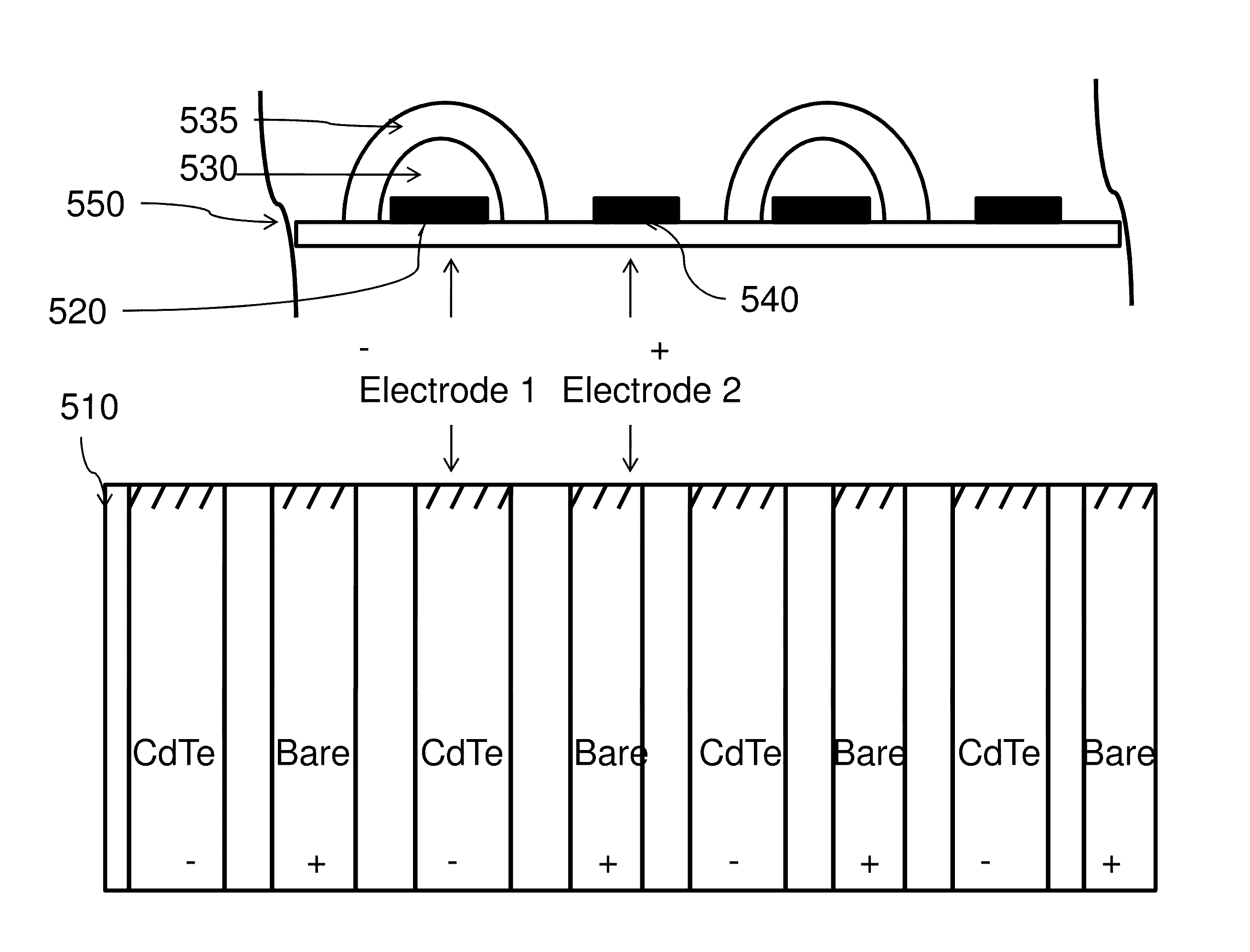
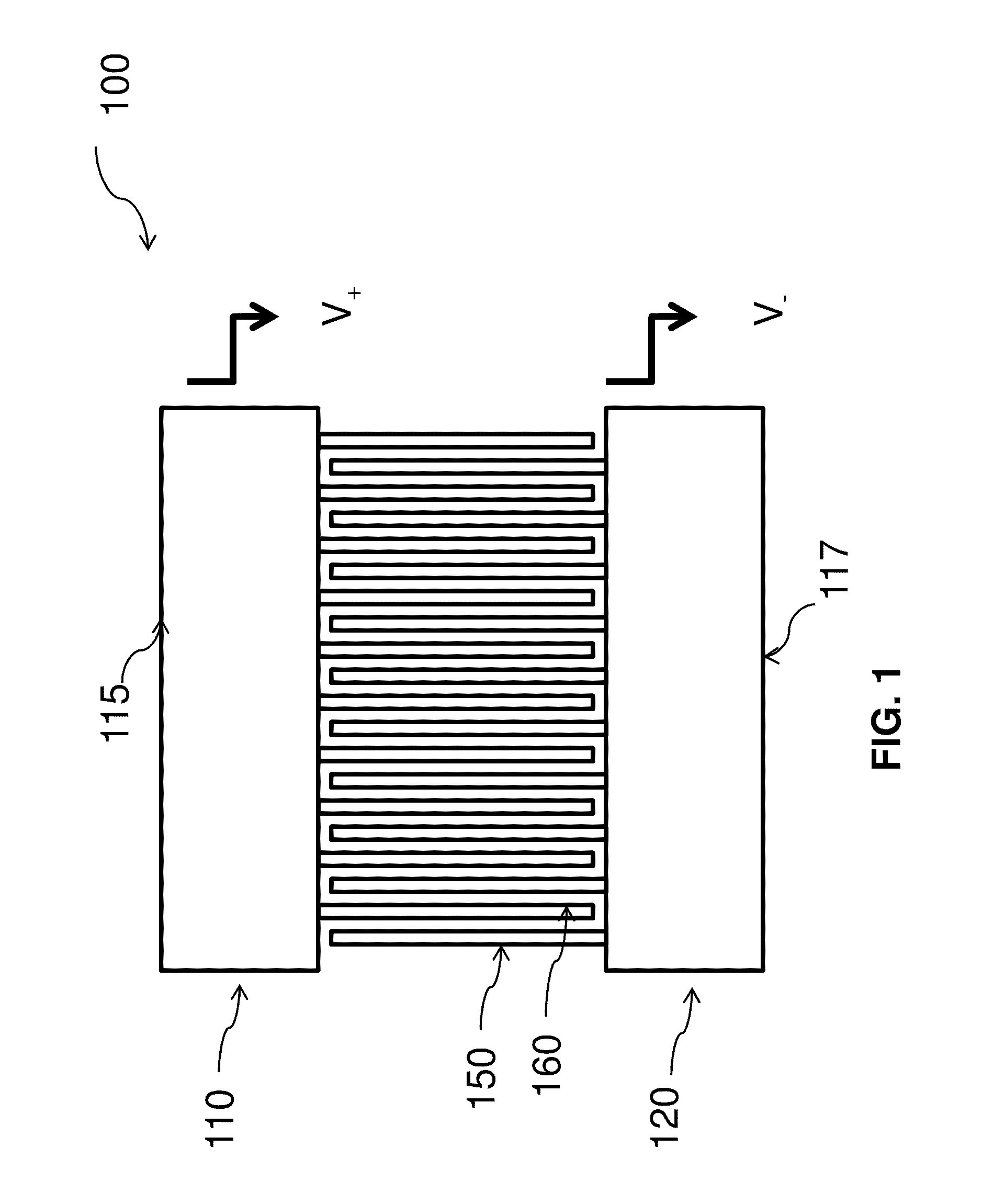
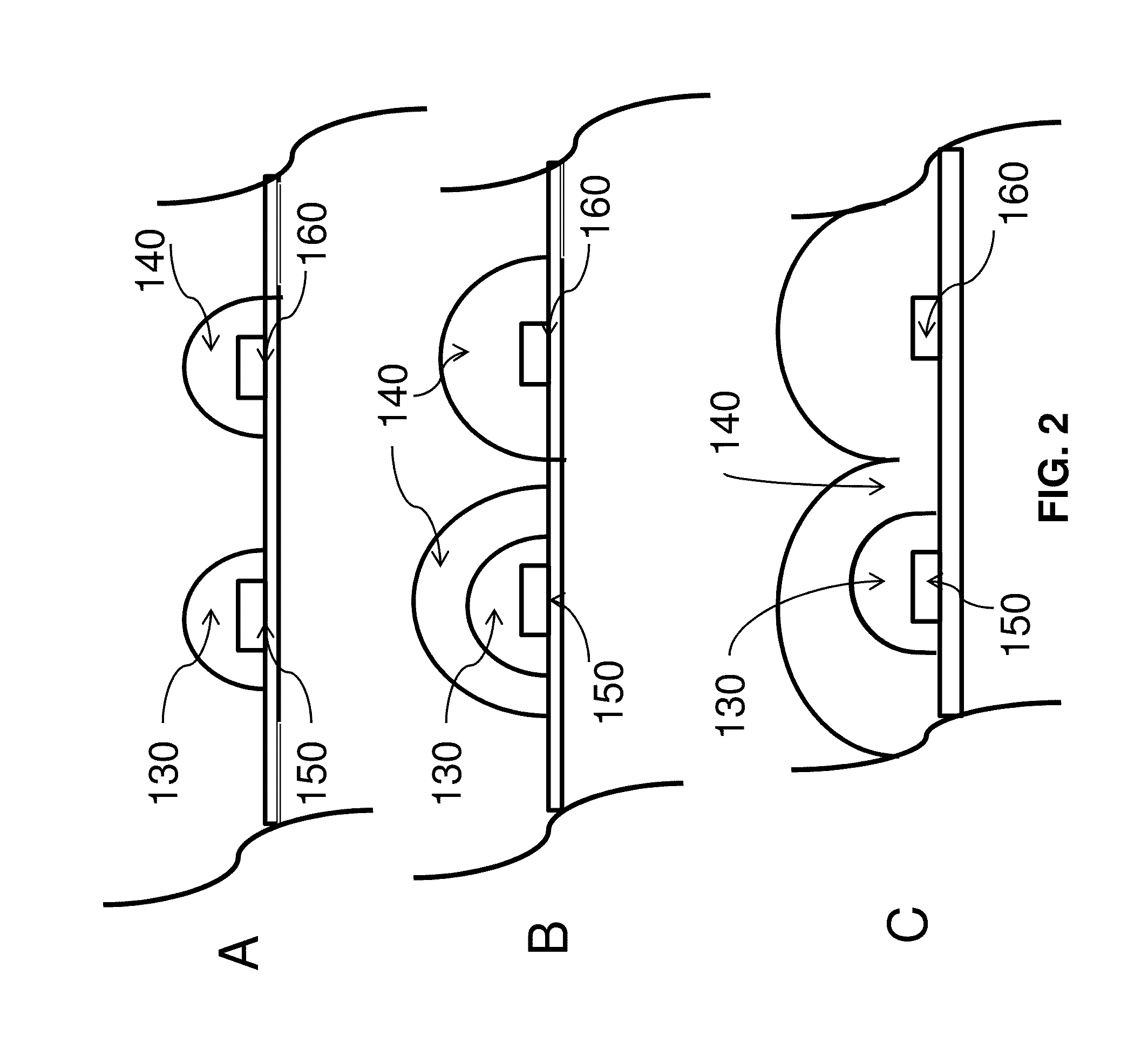
[0047]The present disclosure is directed to three dimensionally structured thin film photovoltaic devices with self-aligned back contacts. Fabrication of this photovoltaic device includes an electrodeposition process on at least one of two or more interdigitated electrodes.

[0048]The electrodeposition process described herein applies to existing technologies for production of interdigitated electrodes to create a new and unobvious self-aligned electrochemical deposition process.

[0049]Interdigitated damascene wires with a pitch below 100 nanometers (nm) are regularly fabricated in interdigitated comb-like electrode structures to study leakage current in microelectronics applications. It is also known to deposit micrometer pitch interdigitated electrodes on top of semiconductors to form metal-semiconductor-metal structures for photodetectors. However, in accordance with the present disclosure, such patterned electrically conducting wires on an insulating substrate may serve as the acti...


PUM


Abstract

A process for producing three dimensionally structured thin film photovoltaic devices with self-aligned back contacts. The photovoltaic device is constructed using electrodeposition on micrometer-scale interdigitated electrodes on an insulating substrate. During fabrication, these interdigitated electrodes serve as the active electrodes for deposition of materials including semiconductors. After fabrication, these interdigitated electrodes serve as back contacts for carrier collection when the device is in use. The process can be used to fabricate homojunction, heterojunction and multijunction photovoltaic devices.

Description

STATEMENT REGARDING FEDERALLY SPONSORED RESEARCH / DEVELOPMENT[0001]The subject matter of this patent application was invented by employees of the United States Government. Accordingly, the United States Government may manufacture and use the invention for governmental purposes without the payment of any royalties.BACKGROUND OF THE INVENTION[0002]1. Field of Invention[0003]The present disclosure relates to photovoltaic devices and, more particularly, to photovoltaic devices produced by an electrochemical deposition process onto two or more electrodes, each including a contact pad and a number of parallel wires connected to the contact pad, the wires of the different electrodes being interdigitated.[0004]2. Description of Related Art[0005]Photovoltaic or solar devices may be used to convert light directly into electrical current. This conversion may be accomplished via the conjunction of n-type and p-type semiconducting materials that separate electron-hole pairs which are created when...

Claims


Application Information

Patent Timeline
IPC IPC(8): H01L31/0224H01L31/06H01L31/18H01L31/068H01L31/072
CPCH01L21/02562Y02E10/547H01L21/02628H01L31/022425H01L31/0236H01L31/0296H01L31/032H01L31/0322H01L31/03529H01L31/068H01L31/072H01L31/0725H01L31/073H01L31/1836Y02E10/541Y02E10/543H01L21/02573Y02P70/50
Inventor JOSELL, DANIELBEAUCHAMP, CARLOS R.MOFFAT, THOMAS P.
Owner GOVERNMENT OF THE UNITED STATES OF AMERICA AS REPRESENTED BY THE SEC OF COMMERCE THE NAT INST OF STANDARDS & TEHCNOLOGY
Why Eureka
Try Eureka