High Voltage Tolerant Input/Output Interface Circuit

a high voltage tolerance, input/output interface technology, applied in the field of electrical and electronic arts, can solve the problems of stacked mos device approach, additional ic fabrication steps, and more area in the ic, so as to improve the tolerance to high voltage signals, increase the voltage tolerance, and add any significant cost

Active Publication Date: 2011-02-24
AVAGO TECH INT SALES PTE LTD
View PDF21 Cites 3 Cited by
  • Summary
  • Abstract
  • Description
  • Claims
  • Application Information

AI Technical Summary

Benefits of technology

[0006]Illustrative embodiments of the invention meet the above-noted need by providing an IO interface circuit having improved tolerance to high voltage signals. Techniques of the present invention beneficially eliminate the need for stacked MOS devices by utilizing one or more parasitic bipolar

Problems solved by technology

This creates a problem for the stacked MOS device approach.
Additionally, utilizing stacked MOS devices requires more area in the IC compared to a non-stacked device

Method used


Image

  • High Voltage Tolerant Input/Output Interface Circuit
  • High Voltage Tolerant Input/Output Interface Circuit
  • High Voltage Tolerant Input/Output Interface Circuit

Examples


Embodiment Construction

[0015]The present invention will be described herein in the context of exemplary IO interface circuits. It is to be understood, however, that the present invention is not limited to the circuits shown and described herein. Rather, embodiments of the invention may be implemented in any application that can benefit from an interface circuit having increased tolerance to high voltage. Although preferred embodiments of the invention may be fabricated in a silicon wafer, embodiments of the invention can alternatively be fabricated in wafers comprising other materials, including but not limited to Gallium Arsenide (GaAs), Indium Phosphide (InP), etc.

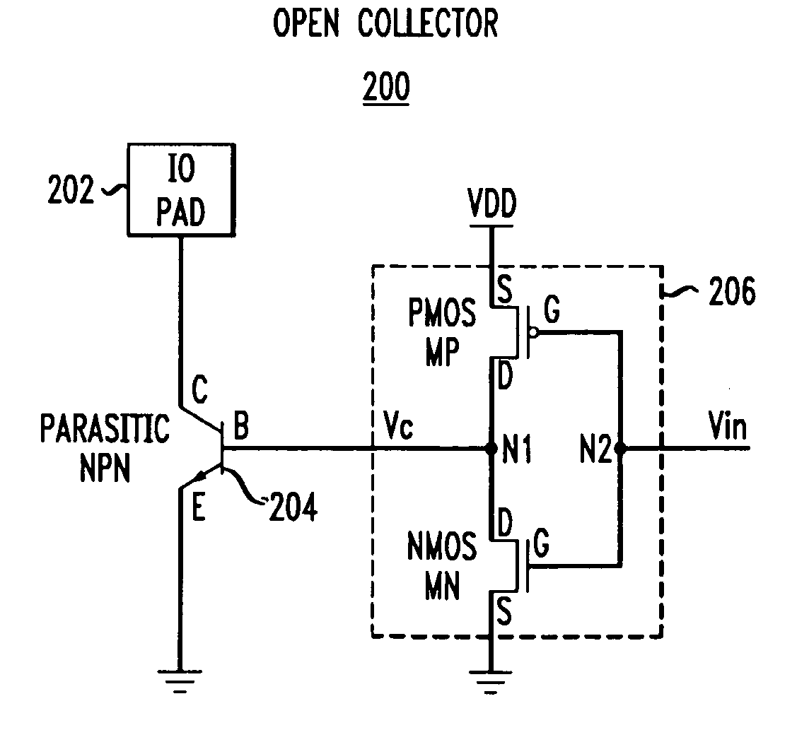
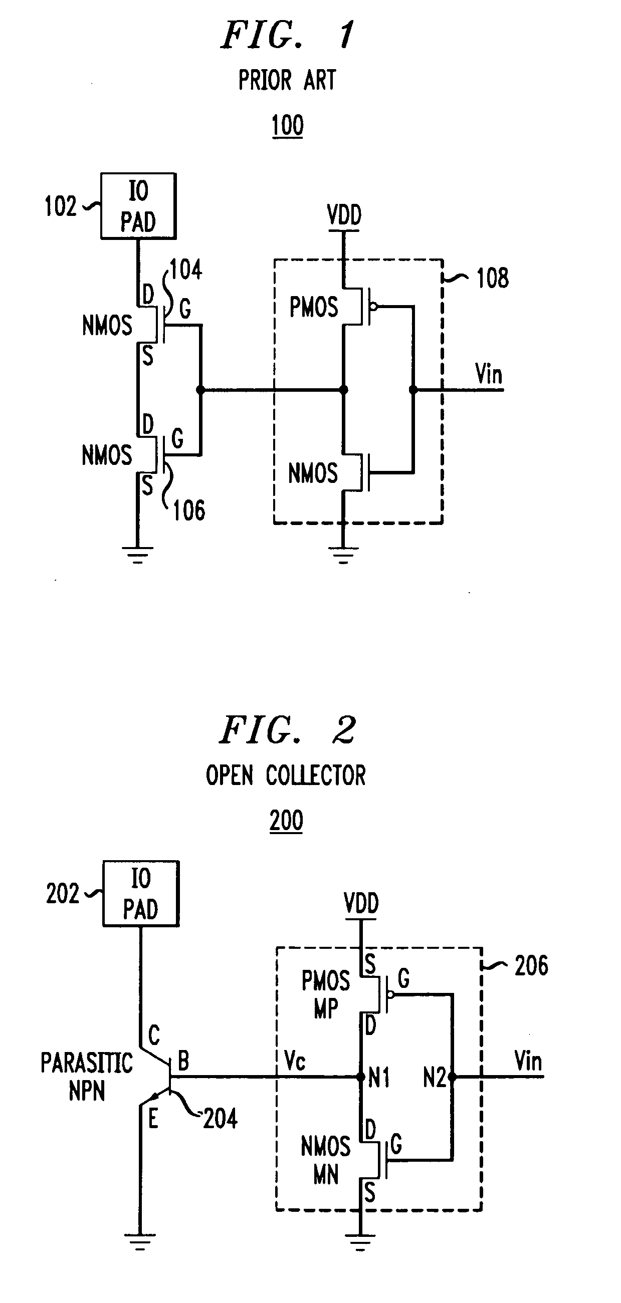
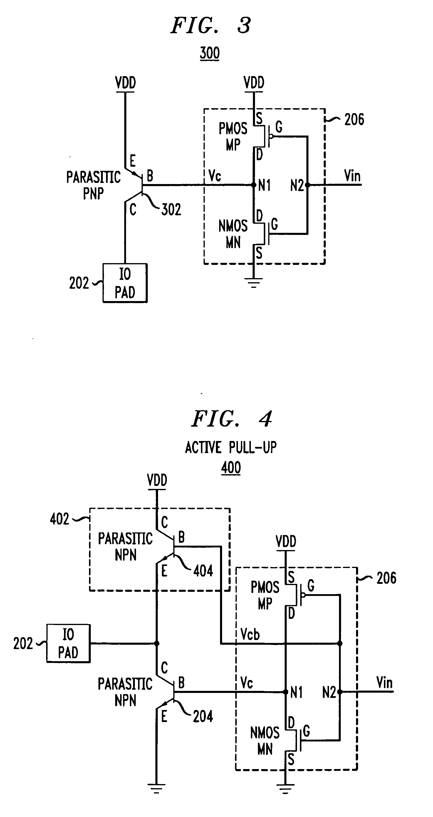
[0016]FIG. 1 is a schematic diagram illustrating at least a portion of a conventional IO interface circuit 100 for use in a high voltage tolerant application. Interface circuit 100 includes an IO pad 102 and an open collector output stage connected to the IO pad, the output stage comprising a pair of stacked n-channel MOS (NMOS) transistor dev...


PUM


Abstract

An IO interface circuit for use in a high voltage tolerant application is provided. The IO interface circuit includes a signal pad and at least a first parasitic bipolar transistor having an emitter adapted for connection to a voltage return of the interface circuit, a base adapted to receive a first control signal, and a collector connected directly to the signal pad in an open collector configuration. The interface circuit further includes a MOS control circuit coupled to the parasitic bipolar transistor and being operative to generate the first control signal. The IO interface circuit may further include an active pull-up circuit connected between a voltage supply of the interface circuit and the signal pad.

Description

FIELD OF THE INVENTION[0001]The present invention relates generally to the electrical and electronic arts, and more particularly relates to input / output (IO) interface circuitry.BACKGROUND OF THE INVENTION[0002]The use of IO interface circuits, such as, for example, IO buffers, is well-known. In advanced complementary metal-oxide-semiconductor (CMOS) integrated circuit (IC) process technology, there has been a push toward lower voltage IO buffers. In a 40 nanometer (nm) IC fabrication process, for example, 1.8-volt transistors are being readily adopted. However, despite the push to utilize lower voltage transistors, there is still a need for high voltage tolerance in certain IO applications that may require interfacing with higher voltages (e.g., 5 volts). One such application is a light emitting diode (LED) driver circuit.[0003]Conventional high voltage tolerant IO interface circuits typically employ stacked metal-oxide-semiconductor (MOS) devices. An example of this configuration ...

Claims


Application Information

Patent Timeline
IPC IPC(8): H03K19/0175H03K3/00
CPCH03K19/00361H03K19/09448H03K19/017518
Inventor HARRIS, EDWARD B.LEUNG, CHE CHOI
Owner AVAGO TECH INT SALES PTE LTD
Why Eureka
Try Eureka