Inspection system and inspection method

a technology of inspection system and inspection method, applied in the direction of originals for photomechanical treatment, image enhancement, instruments, etc., can solve the problems of loss of yield, method cannot detect a defect common to both compared patterns, and new types of mask defects have been encountered

Active Publication Date: 2011-02-24
NUFLARE TECH INC
View PDF6 Cites 22 Cited by
  • Summary
  • Abstract
  • Description
  • Claims
  • Application Information

AI Technical Summary

Problems solved by technology

A major cause of loss in yield is due to defects of a mask pattern.
However, this method cannot detect a defect common to both compared patterns.
As pattern dimensions have been scaled down, new types of mask defects have been encountered.
That is, current problems to be addressed include not only pattern edge irregularities, formation of isolated holes, and adhesion of material, but also subtle pattern line width errors and pattern displacement.
A deviation in the pattern line width or in the spacing between adjacent patterns results in a change in the pattern's impedance and hence a change in the performance of the completed LSI.
However, the repair information conventionally used to repair detected defects is not sufficient to allow the repair system to locate subtle pattern defects without difficulty even if they are detected by the inspection system.
That is, since conventional repair information includes only optical images captured by the inspection system and coordinate data of defects, the repair system may not be able to locate pattern portions, or defects, to be repaired if they have shapes typical of recent fine patterns, which shapes are hard to identify.

Method used


Image

  • Inspection system and inspection method
  • Inspection system and inspection method
  • Inspection system and inspection method

Examples


first embodiment

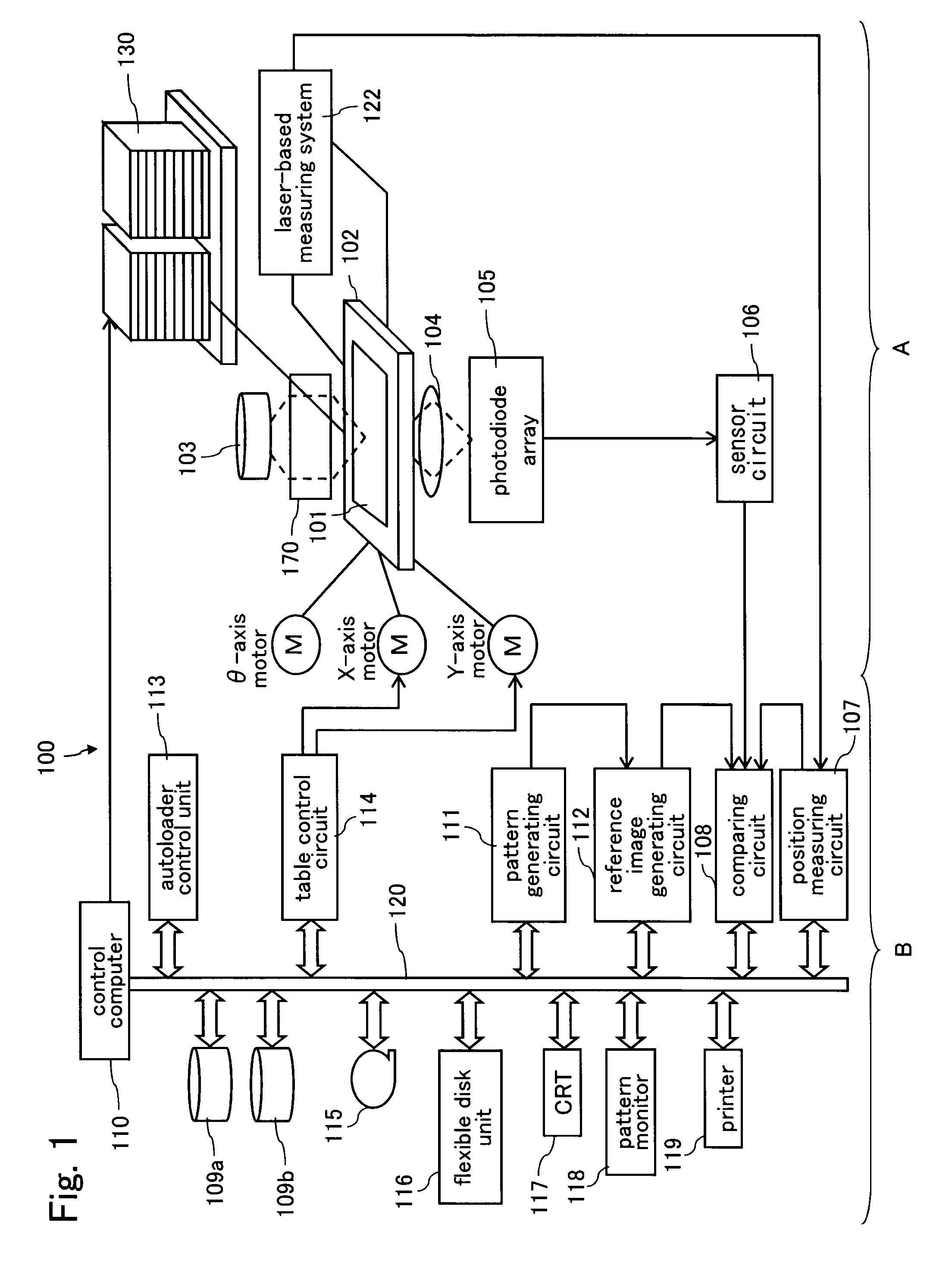
[0024]FIG. 1 is a diagram showing the configuration of an inspection system according to an embodiment of the present invention. Although the inspection system of the present embodiment will be described in connection with the inspection of masks used in photolithography, it is to be understood that the system may be used to inspect wafers.

[0025]As shown in FIG. 1, the mask inspection system 100 includes an optical image capture unit A and a control unit B.

[0026]The optical image capture unit A includes a light source 103, an XYθ table 102 movable in the horizontal X and Y directions and rotatable in a horizontal plane (or in a θ direction), an illumination optical system 170 serving as a transmission illumination system, an enlarging optical system 104, a photodiode array 105, a sensor circuit 106, a laser-based measuring system 122, and an autoloader 130.

[0027]In the control unit B, a control computer 110 which controls the entire mask inspection system 100 is connected through a ...

second embodiment

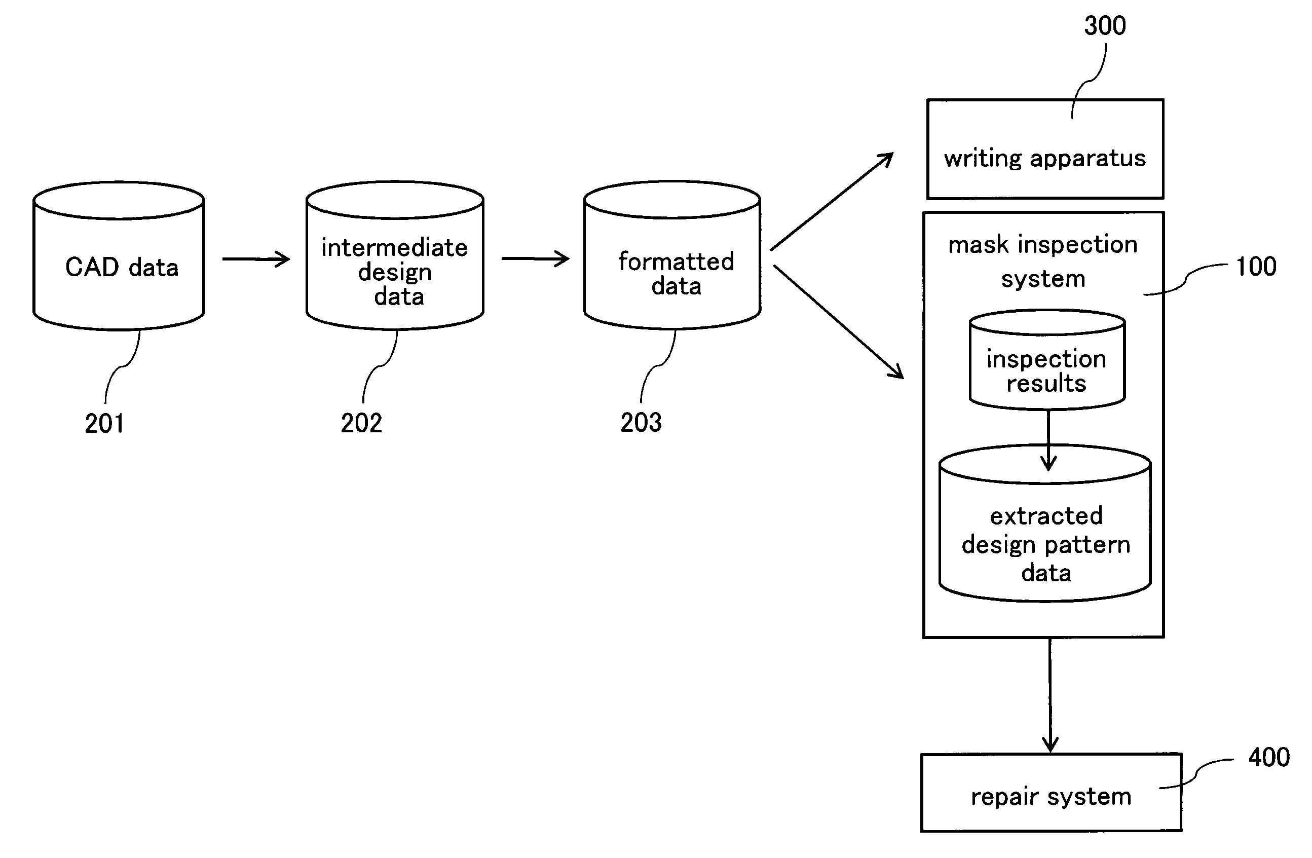
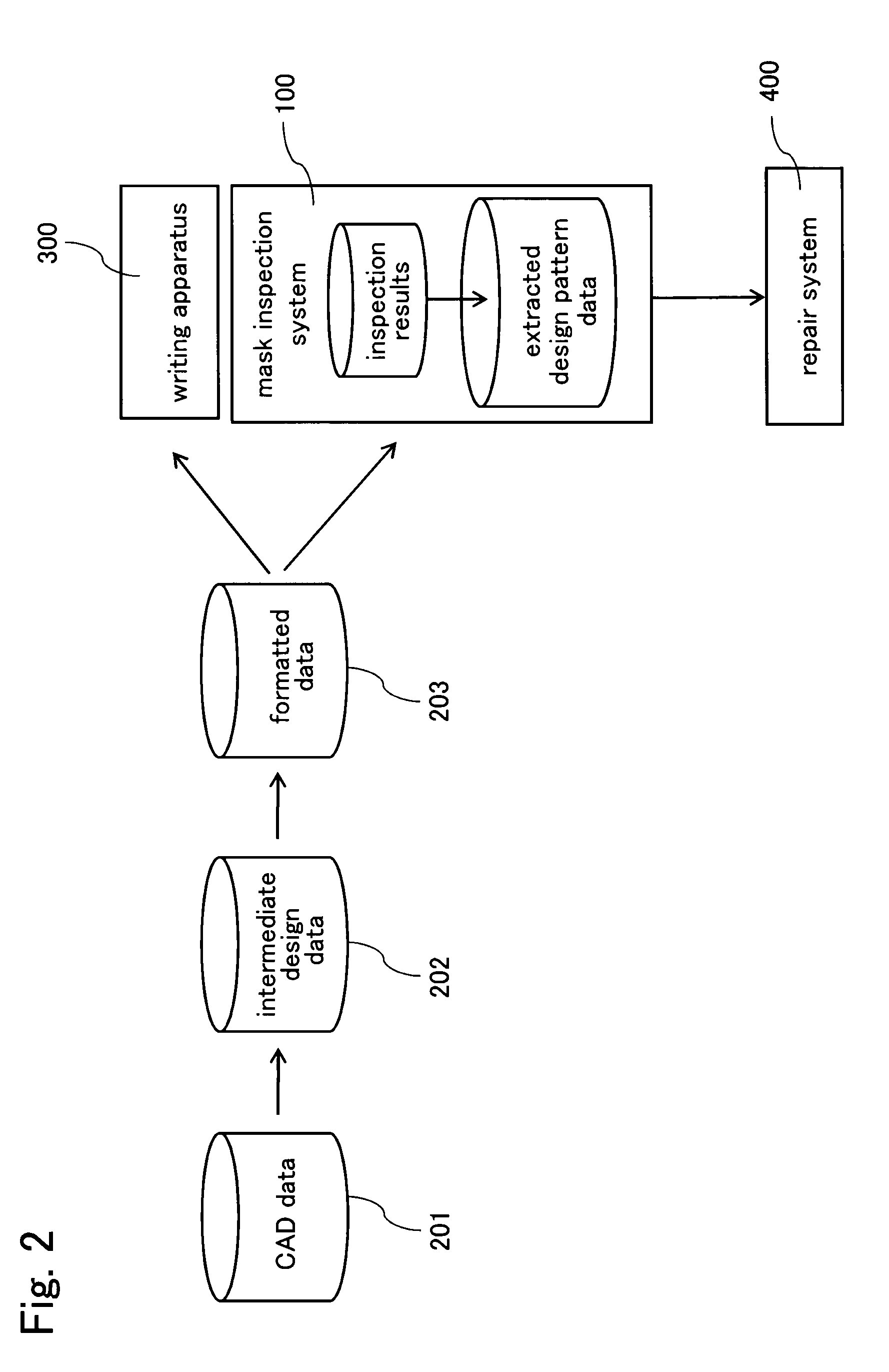
[0057]The inspection system of the first embodiment is adapted to send to the repair system, along with inspection results, an observed sensor image of each defect and databased design pattern data specifying the shape of an area of the pattern around the defect. On the other hand, a second embodiment of the present invention provides an inspection system adapted to send inspection results, etc. to a lithography simulator (or process simulator). It should be noted that the configuration of the inspection system of the present embodiment is the same as that shown in FIG. 1 and described in connection with the first embodiment.

[0058]In recent years, defects associated with micropatterns include not only shape defects typified by pattern edge roughness, but also pattern line width defects and spacing defects between adjacent patterns due to pattern displacement, which are becoming more and more significant. Therefore, there has been an extremely strong need to accurately control the di...

third embodiment

[0067]It is not necessary to accurately control the dimensions, etc. of all the patterns formed on a mask. For example, a dummy feature or pattern, which does not serve for wiring purposes, is sometimes formed in a place where the pattern density is extremely low. No problem is presented even if this dummy feature or pattern has some “pin-hole defect” or edge roughness.

[0068]On the other hand, it is necessary to accurately control the impedance of a pattern through which a clock signal passes (i.e., a clock line), and the position and the diameter of a contact hole passing through a plurality of layers.

[0069]In order to address this problem, a method has been proposed in which the level of importance, or weight, of each pattern is added to design pattern data as pattern importance information, and pattern data and pattern importance information are input to the inspection system. The present invention is also advantageous when applied to inspection systems adapted to use this method...


PUM

PropertyMeasurementUnit
lengthaaaaaaaaaa
opticalaaaaaaaaaa
optical imageaaaaaaaaaa

Abstract

A control computer 110 determines, for each detected pattern defect, a defect inspection pattern area of predetermined X and Y dimensions containing the coordinates of the defect, then determines the clusters or cells whose reference points are located within the defect inspection pattern area. Then extracts the data of these clusters or cells from design pattern data read from a first magnetic disk unit 109a. The control computer 110 then generates an output file containing the extracted data. The output file is then converted into the same format as the input design pattern data or into OASIS format, before it is output to a second magnetic disk unit 109b. The extracted pattern data specifying the clusters or cells within each defect inspection pattern area can be output from the mask inspection system 100 to external systems.

Description

BACKGROUND OF THE INVENTION[0001]1. Field of the Invention[0002]The present invention relates to an inspection system and an inspection method, and more particularly to an inspection system and an inspection method for detecting defects of the pattern formed on an object to be inspected, such as a mask.[0003]2. Background Art[0004]In recent years, as the levels of integration and capacity of large scale integrated circuits (LSIs) increase, there has been a need to continue to reduce the width of the circuit patterns of semiconductor devices. Semiconductor devices are manufactured by a reduced projection exposure apparatus called a “stepper” using original artwork patterns with a circuit pattern formed thereon, that is, masks or reticles (hereinafter referred to collectively as masks). Specifically, the pattern on a mask is transferred to the wafer by exposure to light, thereby forming circuits on the wafer. Masks used to transfer such fine circuit patterns to the wafer are manufactu...

Claims


Application Information

Patent Timeline
Patent Type & Authority Applications(United States)
IPC IPC(8): G06T7/00G01N21/956G03F1/68G03F1/84H01L21/027
CPCG01N21/8851G01N21/95607G06T2207/30148G03F1/84G01N2021/95676
Inventor TSUCHIYA, HIDEOINOUE, TAKAFUMI
Owner NUFLARE TECH INC
Why Eureka
Try Eureka