
Solid-state imaging device and process of making solid state imaging device

a solid-state imaging and imaging device technology, applied in the field the making of solid-state imaging devices, can solve the problems of reducing the effective area of the photodiode, the reduction of the aperture ratio, and the reduction of the pixel aperture ratio, so as to reduce the dark current, improve the sn ratio, and prevent color cross-talk

Active Publication Date: 2011-03-03
FUJIFILM CORP
View PDF10 Cites 44 Cited by
  • Summary
  • Abstract
  • Description
  • Claims
  • Application Information

AI Technical Summary

Benefits of technology

[0214]If desired, the colored thermosetting composition may contain various additives as long as such does not affect the effects of the invention. Examples of additives include binders, curing agents, curing catalysts, solvents, fillers, polymeric compounds other than those described, surfactants, adhesion enhancer, antioxidants, UV absorbers, anti-coagulants, and dispersants.

Problems solved by technology

Therefore, as the pixel pitch reduces, the area ratio of the circuit region in unit pixel becomes larger, which of necessity raises the problem of reduction in the effective area of the photodiode, i.e., reduction of a pixel aperture ratio.
Reduction of aperture ratio leads to reduction of sensitivity.

Method used


Image

  • Solid-state imaging device and process of making solid state imaging device
  • Solid-state imaging device and process of making solid state imaging device
  • Solid-state imaging device and process of making solid state imaging device

Examples


Embodiment Construction

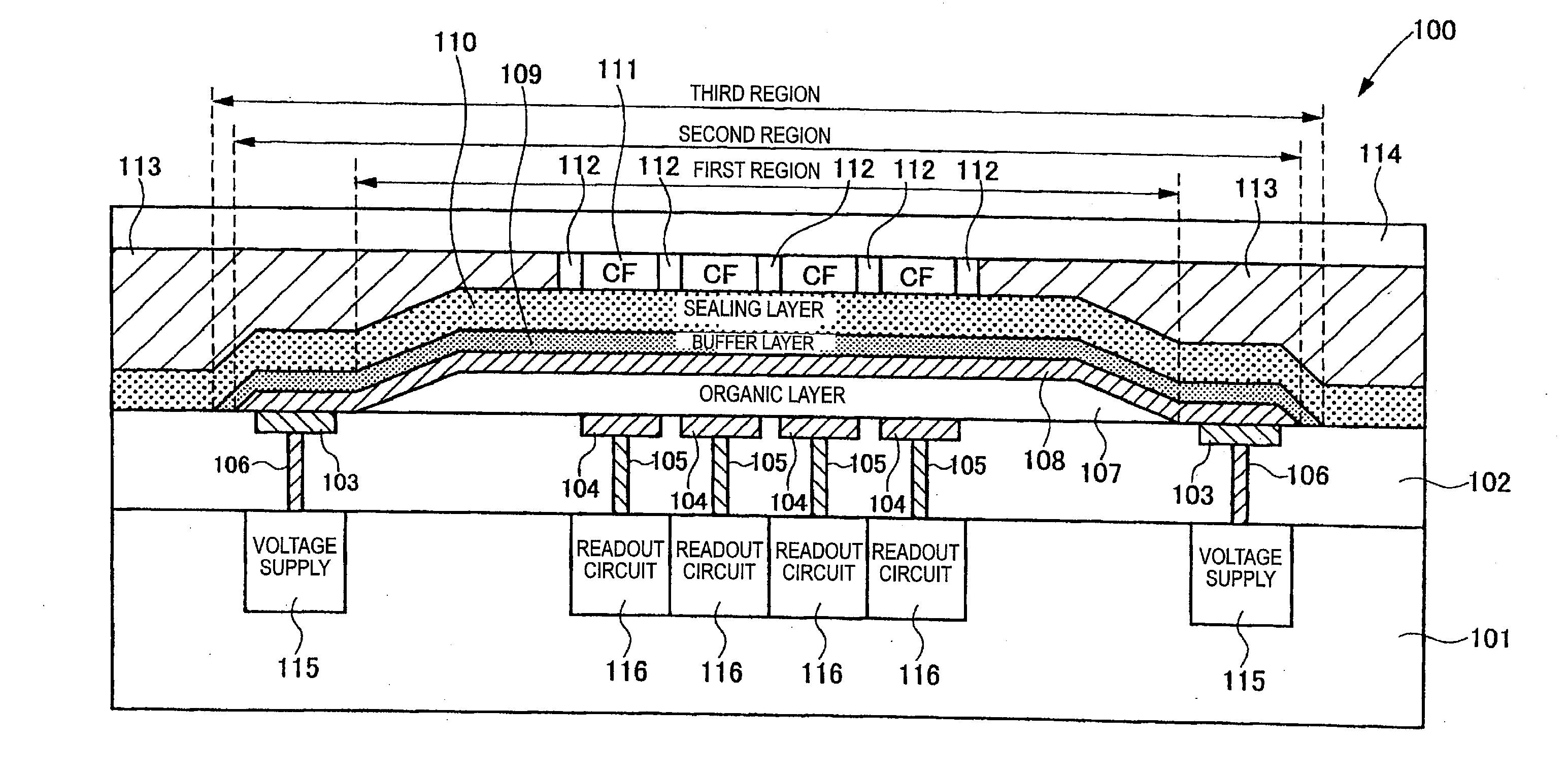
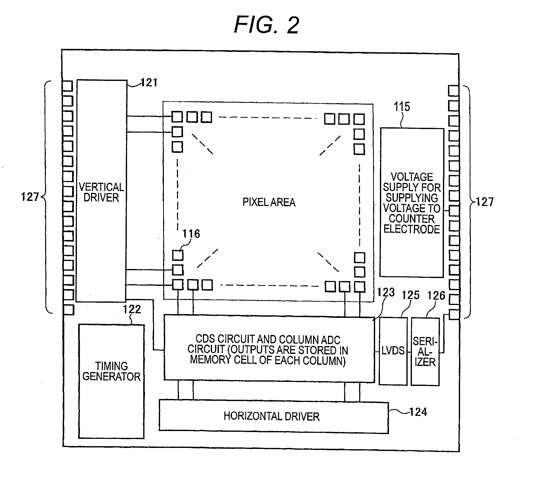
[0068]FIG. 1 is a schematic cross-section showing the structure of a tandem solid state imaging device 100.

[0069]The solid state imaging device 100 illustrated in FIG. 1 includes a substrate 101, a dielectric layer 102, connection electrodes 103, pixel electrodes 104, vertical interconnects 105, vertical interconnects 106, an organic layer 107, a counter electrode 108, a buffer layer 109, a sealing layer 110, color filters 111, partition walls 112, a light-shielding layer 113, a protective layer 114, a voltage supply 115 for supplying voltage to common electrode, and readout circuits 116.

[0070]The substrate 101 is a glass substrate or a semiconductor (e.g., Si) substrate. The dielectric layer 102 is formed on the substrate 101. A plurality of pixel electrodes 104 and a plurality of connection electrodes 103 are formed in the surface portion of the dielectric layer 102.

[0071]The organic layer 107 contains at least a photoelectric layer that generates charges in response to light rece...


PUM


Abstract

A solid state imaging device includes an array of pixels, each of the pixels includes: a pixel electrode; an organic layer; a counter electrode; a sealing layer; a color filter; and a readout circuit as defined herein, the photoelectric layer contains an organic p type semiconductor and an organic n type semiconductor, an ionization potential of the charge blocking layer and an electron affinity of the organic n type semiconductor in the photoelectric layer have a difference of at least 1 eV, and the solid-state imaging device further includes a transparent partition wall between adjacent color filters of adjacent pixels of the array of pixels, the partition wall being made from a transparent material having a lower refractive index than a material forming the color filters.

Description

FIELD OF THE INVENTION[0001]This invention relates to a solid-state imaging device, and a method of making a solid state imaging device.BACKGROUND OF THE INVENTION[0002]As image sensors mounted on digital still cameras, digital video cameras, mobile phone cameras, and endoscope cameras, solid state imaging apparatus called CCD sensors or CMOS sensors which include a substrate, e.g., a silicon chip, and an array of pixels containing a photodiode and read out signal charge corresponding to photoelectrons generated in the photodiode of each pixel by a CCD or CMOS readout circuit are known.[0003]The known solid state imaging apparatus includes not only the photodiode but a signal readout circuit and an accompanying multilevel interconnect formed on the semiconductor substrate for every pixel. Therefore, as the pixel pitch reduces, the area ratio of the circuit region in unit pixel becomes larger, which of necessity raises the problem of reduction in the effective area of the photodiode,...

Claims


Application Information

Patent Timeline
Patent Type & Authority Applications(United States)
IPC IPC(8): H01L31/0232H01L31/18H10K99/00
CPCH01L27/14609H01L27/14625H01L27/14629H01L27/14645H01L27/14687Y02E10/549H01L27/307H01L51/0053H01L51/0059H01L51/4273H01L27/14692Y02P70/50H10K39/32H10K85/621H10K85/631H10K30/353
Inventor MAEHARA, YOSHIKIGOTO, TAKASHISUZUKI, HIDEYUKISAWAKI, DAIGO
Owner FUJIFILM CORP
Learn More