Method of manufacturing patterned subtrate for culturing cells, patterned subtrate for culturing cells, patterning method of culturing cells, and patterned cell chip

Inactive Publication Date: 2011-03-03
SUNGKYUNKWAN UNIVERSITY
View PDF4 Cites 60 Cited by
  • Summary
  • Abstract
  • Description
  • Claims
  • Application Information

AI Technical Summary

Benefits of technology

[0016]It is still another object of the present invention to provide a patterning method for culturing cells, which is capable of selectively culturing a small amount of cells in the desired position using the patterned substrate for culturing cells.
[0017]

Problems solved by technology

There are several drawbacks associated with cell chips of which the most general one is that cells are not cultured well on a substrate.
On the other hand, when cells are not cultured properly on the substrate, the cells fail to grow and divide.
Second, when cells are cultured on the substrate, their intrinsic properties or organization have to be well maintained.
If

Method used


Image

  • Method of manufacturing patterned subtrate for culturing cells, patterned subtrate for culturing cells, patterning method of culturing cells, and patterned cell chip
  • Method of manufacturing patterned subtrate for culturing cells, patterned subtrate for culturing cells, patterning method of culturing cells, and patterned cell chip
  • Method of manufacturing patterned subtrate for culturing cells, patterned subtrate for culturing cells, patterning method of culturing cells, and patterned cell chip

Examples


preparation example 1

Formation of First Plasma Polymer Layer on Substrate

[0076]A plasma polymerized hexamethyldisiloxane (PPHMDSO) thin film prepared by plasma enhanced chemical vapor deposition using hexamethyldisiloxane as a first precursor material was deposited on a glass slide having a size of 75 mm×25 mm (Corning Microslide Plain, Cat#: 2947, Corning, N.Y.).

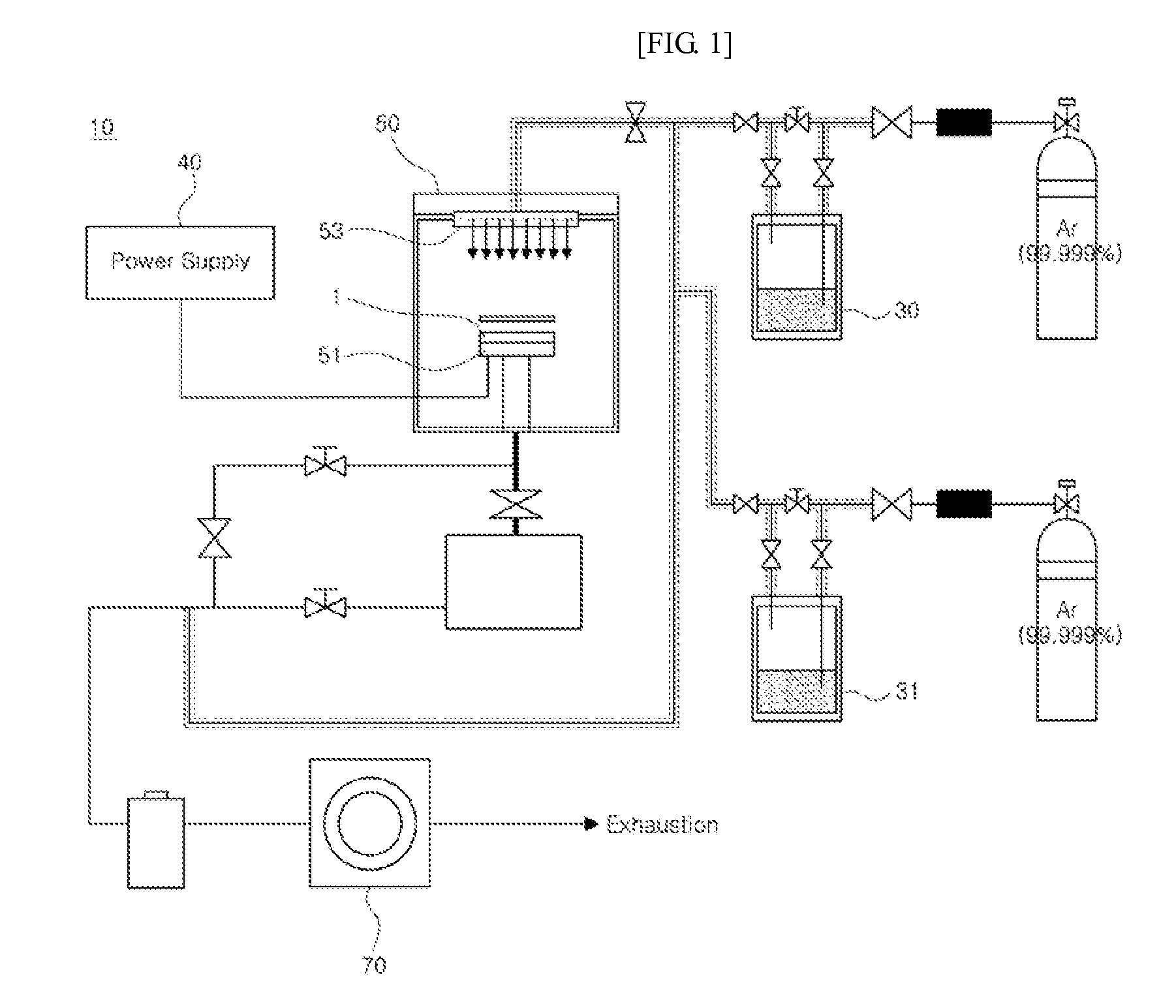
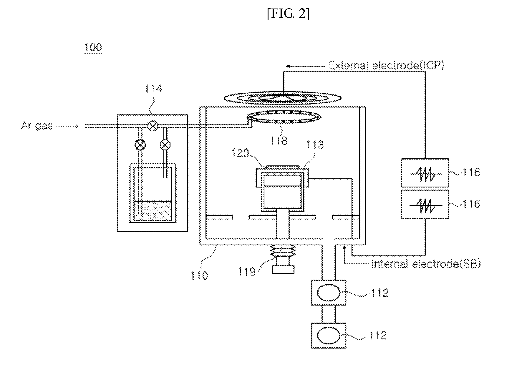
[0077]Specifically, the deposition was performed using the plasma enhanced chemical vapor deposition apparatus depicted in FIG. 1. The plasma reaction chamber 50 has a cylindrical shape and is constructed of stainless material. Hexamethyldisiloxane monomer was placed into the bubbler 30, 31 which was heated at 50° C. Hexamethyldisiloxane molecule was vaporized by using an inert gas of argon as a carrier gas and injected into the plasma reaction chamber 50. SB power was supplied to attach the rf generator to a slide substrate holder 51 to generate plasma around the slide. Here, the wall surface of the plasma reaction chamber 50 was put to earth....

preparation example 2

Formation of First Plasma Polymer Layer on Substrate

[0078]A substrate having a first plasma polymer layer, in which a plasma polymerized hexamethyldisiloxane thin film was deposited on a glass slide, was manufactured in the same manner as in Preparation Example 1, except that the internal electrode (SB) of the plasma reaction chamber 50 was maintained at 30 W in Preparation Example 2.

preparation example 3

Formation of First Plasma Polymer Layer on Substrate

[0079]A substrate having a first plasma polymer layer, in which a plasma polymerized hexamethyldisiloxane thin film was deposited on a glass slide, was manufactured in the same manner as in Preparation Example 1, except that the internal electrode (SB) of the plasma reaction chamber 50 was maintained at 50 W in Preparation Example 3.


PUM


Abstract

The present invention relates to a method of manufacturing a patterned substrate for culturing cells, comprising the steps of: (1) preparing a substrate; (2) forming a first plasma polymer layer by integrating a first precursor material using a plasma on the substrate; (3) placing a shadow mask having a predetermined pattern on the first plasma polymer layer; and (4) forming a second patterned plasma polymer layer by integrating a second precursor material using a plasma.

Description

BACKGROUND OF THE INVENTION[0001]1. Field of the Invention[0002]The present invention relates to a method of manufacturing a patterned substrate for culturing cells, a patterned substrate for culturing cells, a patterning method for culturing cells, and a cell chip; and more particularly, a method of manufacturing a patterned substrate for culturing cells, a patterned substrate for culturing cells, a patterning method for culturing cells, and a cell chip, in which a substrate capable of inhibiting cell adsorption is manufactured using a plasma and cells are selectively cultured by patterning and integrating many numbers of functional groups on the substrate.[0003]2. Description of the Related Art[0004]Research relating to human life such as the human genome project is rapidly increasing. Information analysis and understanding of the operation of living organisms are gathering strength with ongoing research on living organisms. Accordingly, interest in biochips for rapid analysis of ...

Claims


Application Information

Patent Timeline
IPC IPC(8): C40B40/02B05D5/00C40B60/14C40B50/06
CPCB01J2219/00509B01J2219/00527B01J2219/00605B01J2219/00612B01J2219/00614B01J2219/00619C12N2535/10B01J2219/00635B01J2219/00637B01J2219/00743C12N5/0068C12N2533/12C12N2533/30B01J2219/00621C12M3/00C12N5/00G01N33/48
Inventor JUNG, DONG GEUNCHOI, CHANG ROKKIM, KYUNG SEOP
Owner SUNGKYUNKWAN UNIVERSITY
Why Eureka
Try Eureka