Organic light-emitting device

a light-emitting device and organic technology, applied in the field of organic semiconductor devices, can solve problems such as the deterioration of contrast of the panel at a light-pla

Inactive Publication Date: 2011-03-17
PIONEER CORP
View PDF5 Cites 48 Cited by
  • Summary
  • Abstract
  • Description
  • Claims
  • Application Information

AI Technical Summary

Benefits of technology

[0012]Due to the above configuration of the invention, the light-scattering layer is introduced into the device; it reduces an interference effect so that settings of elements are allowed in a status unrestricted re...

Problems solved by technology

In an organic EL display apparatus, there may be a contrast deterioration of the panel at a light-p...

Method used


Image

  • Organic light-emitting device
  • Organic light-emitting device
  • Organic light-emitting device

Examples


example np

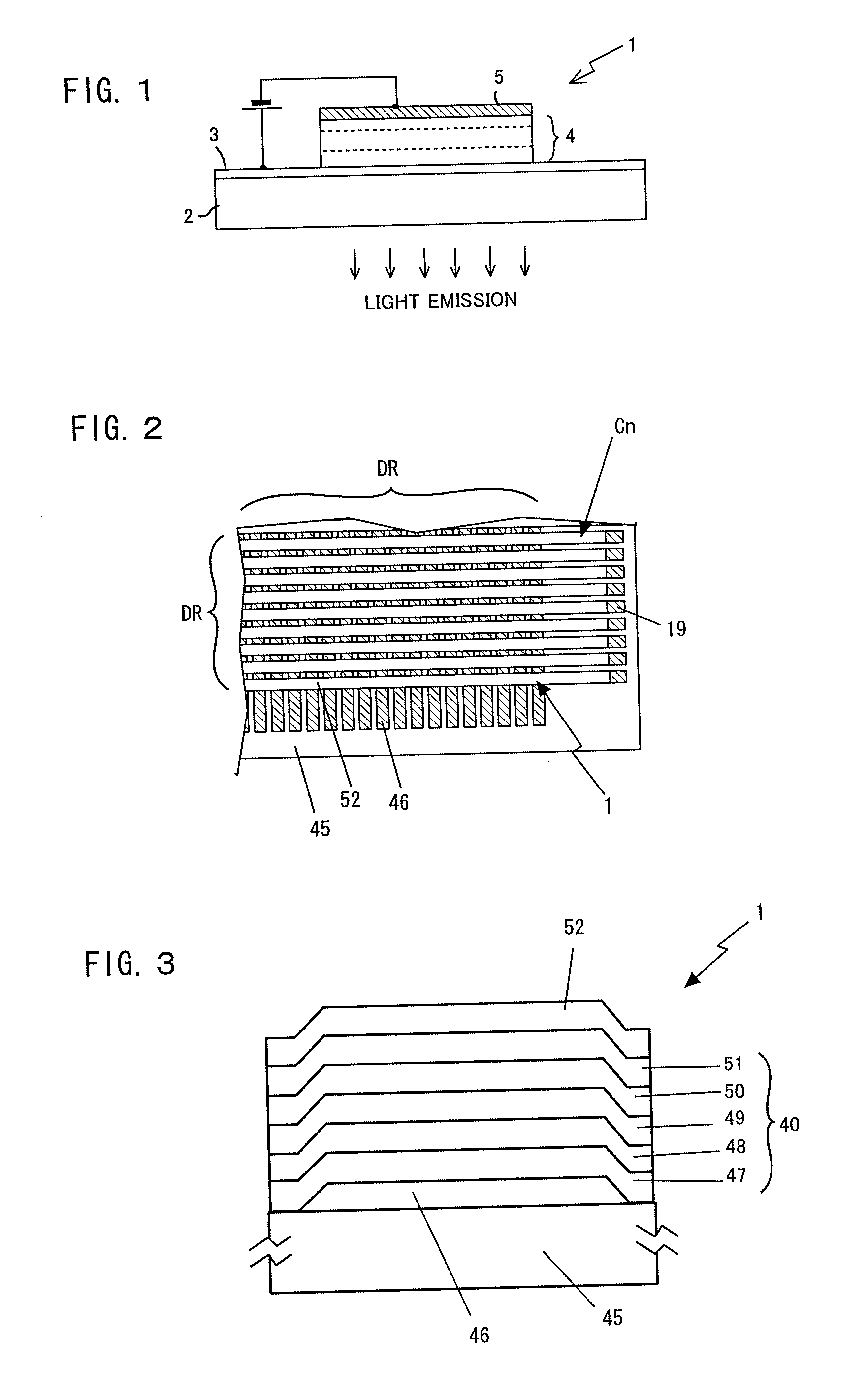
[0058]FIG. 5 is a schematic image diagram showing a cross-section of an organic light-emitting device of Example NP for explaining typical optical paths. In the figure, gaps are drawn between the layers, since only the figure of being easily observed is taken into consideration. The organic light-emitting device 1 has a configuration, on the glass substrate, the transparent anode 46, the light-scattering layer 47a of the hole injection layer in which plural particles are dispersed, the hole transport layer 48, the light-emitting layer 49, the electron transport layer 50, the electron injection layer 51 and the metal cathode 52 are layered in turn. The light-scattering layer 47a is a thin film comprising a base material of the hole injection layer prepared to have a transmittance and to reflect partially light; and particles dispersed therein. The particles are, for example, metal nanoparticles of a metal such as Au, Ag or the like, or an oxide such as TiOx, ZrOx, ZnOx, MoOx, WOx, Si...

example bl

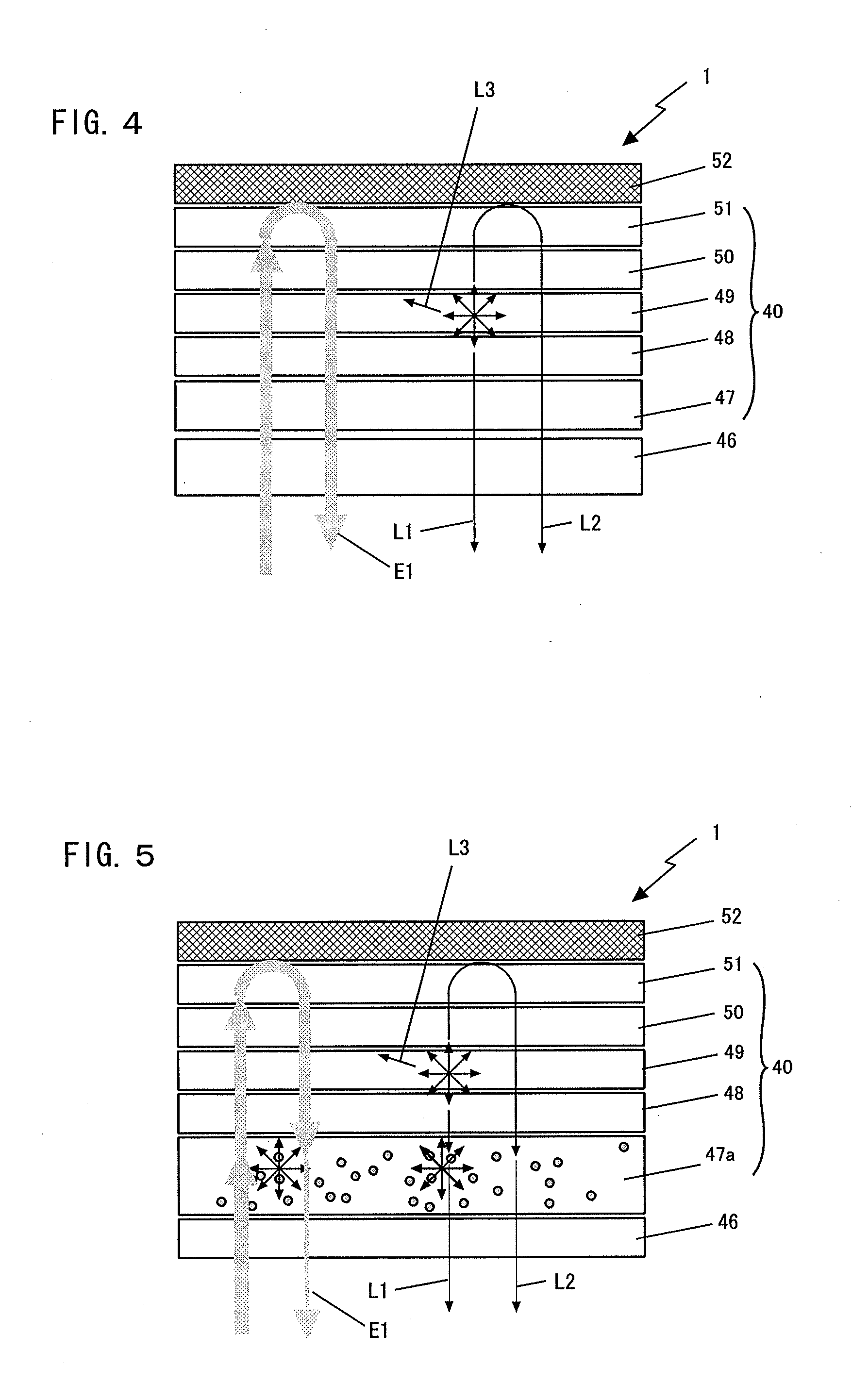
[0061]FIG. 6 is a schematic image diagram showing a cross-section of an organic light-emitting device of Example BL for explaining typical optical paths. In the figure, gaps are drawn between the layers, since only the figure of being easily observed is taken into consideration. The organic light-emitting device 1 has a configuration, on the glass substrate, the transparent anode 46, the hole injection layer 47, the semi-transparent metal layer 99, the hole transport layer 48, the light-emitting layer 49, the electron transport layer 50, the electron injection layer 51 and the metal cathode 52 are layered in turn. The semi-transparent metal layer 99 is formed between the hole injection layer 47 and the hole transport layer 48. The semi-transparent metal layer 99 may be at least one thin film prepared to have a transmittance and to reflect light partially, for example, Ag and MoO3 are contained therein. In addition, the semi-transparent metal layer 99 may be, for example, silver allo...

example bl1

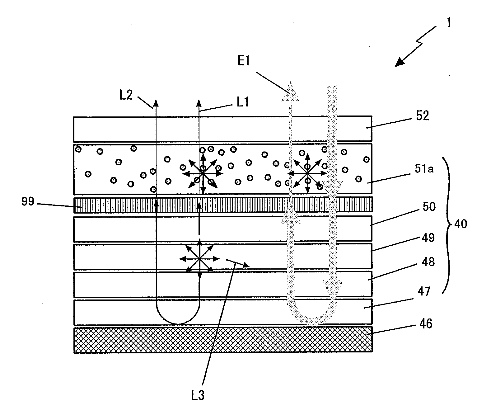
[0065]FIG. 7 is a schematic image diagram showing a cross-section of an organic light-emitting device of Example BL1 for explaining typical optical paths. In the figure, gaps are drawn between the layers, since only the figure of being easily observed is taken into consideration. The organic light-emitting device 1 has a configuration, on the glass substrate, the transparent anode 46, the light-scattering layer 47a of the hole injection layer in which plural particles are dispersed, the semi-transparent metal layer 99, the hole transport layer 48, the light-emitting layer 49, the electron transport layer 50, the electron injection layer 51 and the metal cathode 52 are layered in turn. Example BL1 of the organic light-emitting device has a configuration so that the semi-transparent metal layer 99 (disposed between the light-scattering layer 47a and the hole transport layer 48) is added to FIG. 5's Example NP of the organic light-emitting device having the light-scattering layer 47a. ...


PUM

PropertyMeasurementUnit
Thicknessaaaaaaaaaa
Thicknessaaaaaaaaaa
Lengthaaaaaaaaaa

Abstract

An organic light-emitting device cutting off ambient light while keeping emission intensity includes a pair of first and second electrodes opposed to each other; and a plurality of organic semiconductor layers layered and disposed between the first and second electrodes, wherein the organic semiconductor layers include an organic light-emitting layer, the organic semiconductor device further comprising a light-scattering layer layered and disposed between the organic light-emitting layer and at least one of the first and second electrodes. The light-scattering layer includes: organic materials having carrier injection and transport characteristics of transporting electrons and/or holes; and plural particles dispersed among the organic materials so that light emitted from the organic light-emitting layer is passed therethrough.

Description

TECHNICAL FIELD[0001]The present invention relates to one of organic semiconductor devices, which utilizes an organic compound which exhibits electroluminescence (hereinafter referred to as EL) when electric current is caused to flow thereinto, and particularly an organic light-emitting device comprising an organic light-emitting layer made of such an EL organic compound.BACKGROUND ART[0002]In general, while an organic light-emitting device using an EL organic compound material is an electric current-injection type device having characteristics of a diode. There has been developed a display panel comprising organic light-emitting devices that emit light of two or more luminescent colors and are laid out in a matrix form.[0003]As shown in FIG. 1, each of the organic light-emitting devices 1 is composed of e.g., on a transparent substrate 2, a transparent anode 3, plural organic compound material layers 4 including a light-emitting layer, and a reflective metallic cathode 5, which are...

Claims


Application Information

Patent Timeline
IPC IPC(8): H01L51/52
CPCB82Y20/00B82Y30/00H01L51/0037H05B33/22H01L51/5268H01L2251/5369H01L51/5088C03C17/38C03C2217/445C03C2217/479C03C2217/48C03C2217/948H10K85/1135H10K50/17H10K50/854H10K2102/331
Inventor OYAMADA, TAKAHITO
Owner PIONEER CORP
Why Eureka
Try Eureka