

3D polysilicon diode with low contact resistance and method for forming same
a polysilicon diode and low contact resistance technology, applied in the field of data storage technology, can solve the problems of high forward bias current, and inability to withstand high curren
- Summary
- Abstract
- Description
- Claims
- Application Information
AI Technical Summary
Problems solved by technology
Method used
Image

Examples
Embodiment Construction
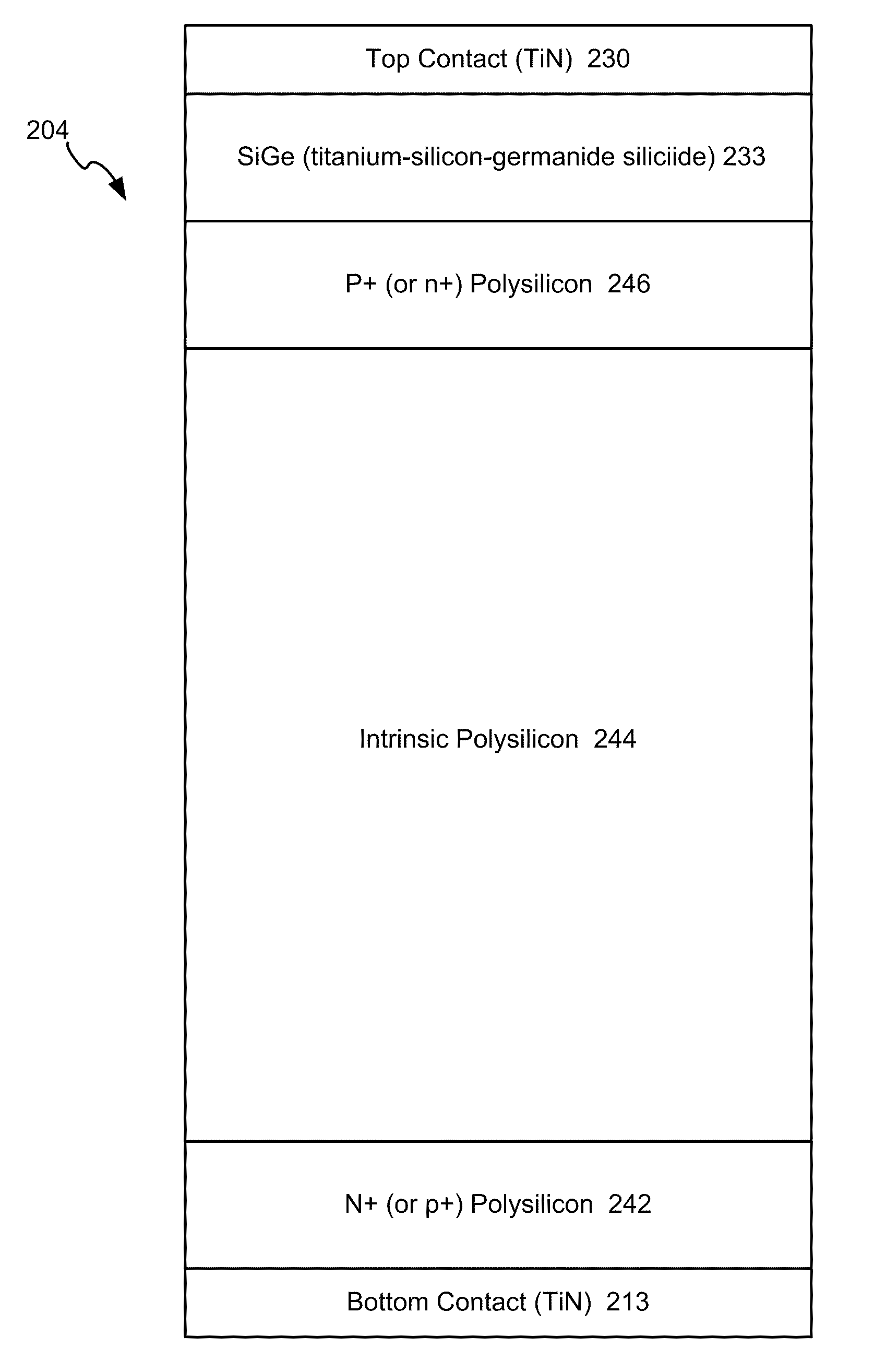
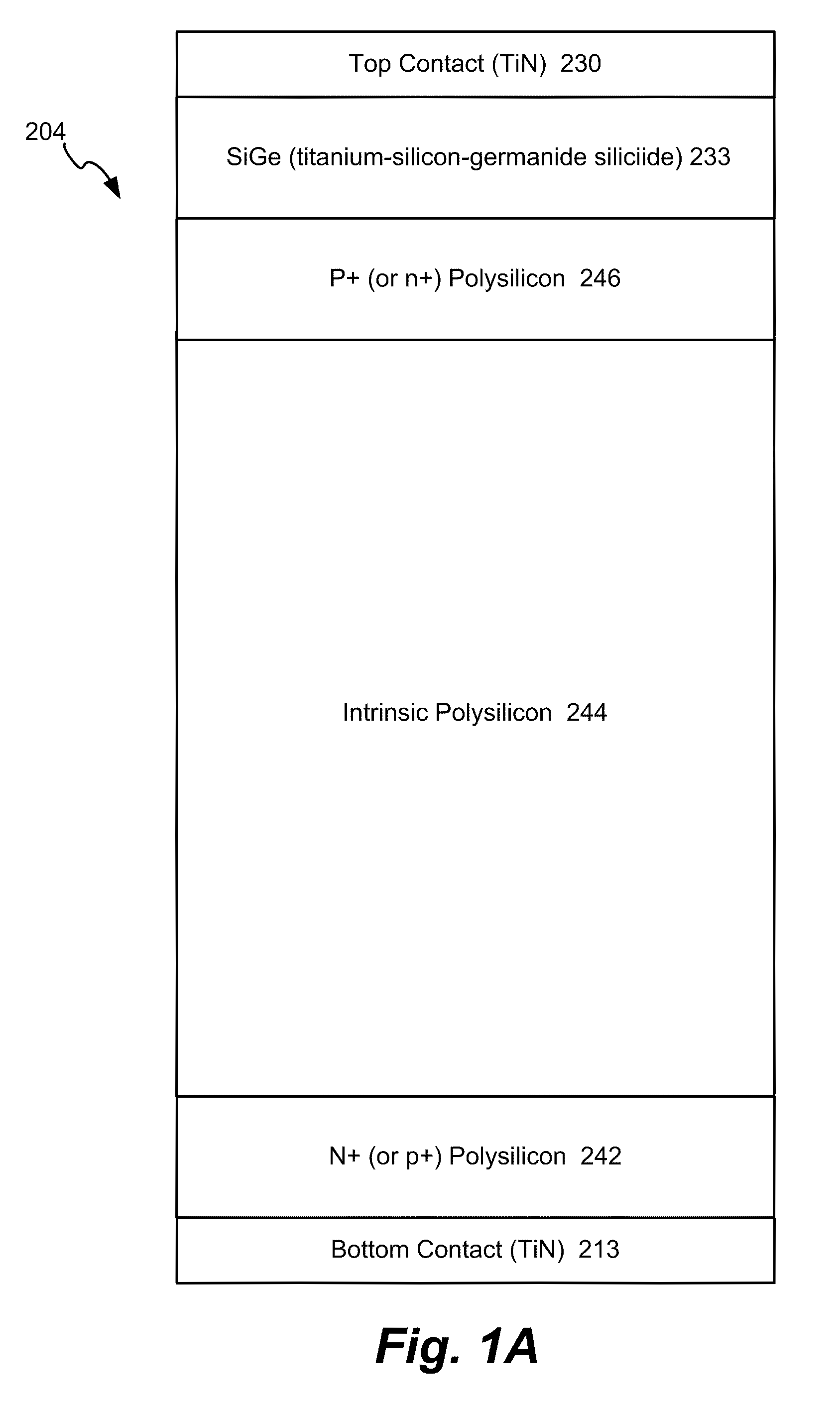
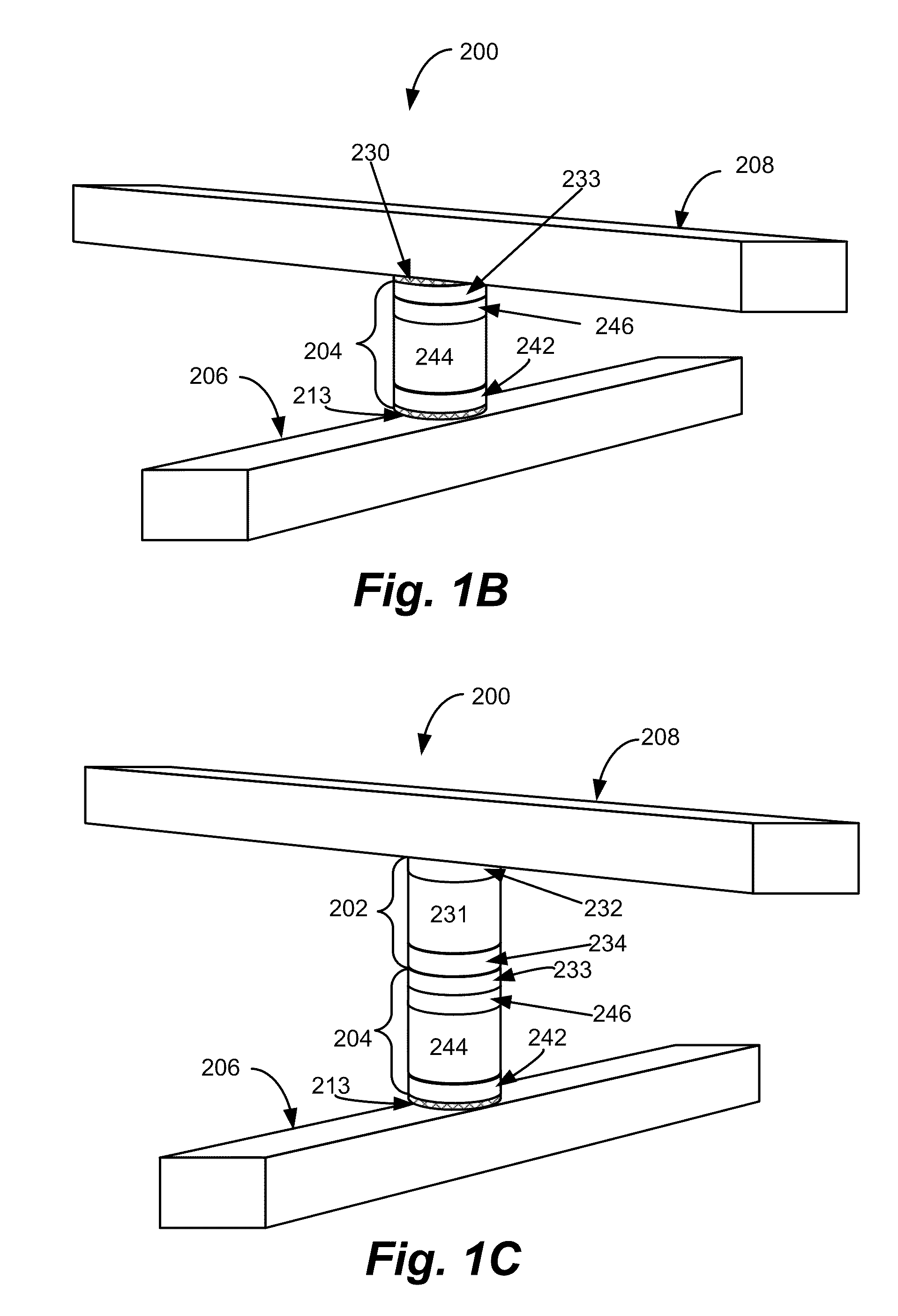
A semiconductor p-i-n diode and method for forming the same are described herein. Memory arrays having p-i-n diodes and techniques for forming memory arrays having p-i-n diodes are disclosed herein. Techniques disclosed herein provide for a low contact resistance between the p-i-n diode and a top contact, which provides for a good forward bias current. Techniques also provide for a relatively low reverse bias current. Thus, the p-i-n diode has a good rectification ratio. Moreover, techniques disclosed herein provide for forming p-i-n diodes in a memory array such that the forward bias currents substantially match. Specifically, the forward bias currents of up-pointing diodes can be made to substantially match those of down pointing diodes, which may achieve better switching results when used in a 3-D memory array. Having the electrical performance of the up- and down-pointing diodes match can obtain better switching yields of the programmed bits at different levels of the memory arr...
PUM
 Abstract
Description
Claims
Application Information