Package substrate

a technology of packaging substrate and substrate, applied in the direction of printed circuit stress/warp reduction, semiconductor/solid-state device details, printed circuit aspects, etc., can solve the problems of increasing the cost of the substrate, affecting the plating area, and requiring the use of additional members

Inactive Publication Date: 2011-03-24
SAMSUNG ELECTRO MECHANICS CO LTD
View PDF10 Cites 9 Cited by
  • Summary
  • Abstract
  • Description
  • Claims
  • Application Information

AI Technical Summary

Benefits of technology

[0015]Accordingly, the present invention has been made keeping in mind the problems encountered in the related art and the present invention is intended to provide a package substrate in which the plating areas of plating layers formed on layers of the package substrate are balanced, so that warpage due to differences in the coefficient of thermal expansion of the plating layers is able to be minimized.

Problems solved by technology

However, the conventional package substrate having a coreless structure has weaker strength compared to a structure using a core substrate, and thus it may easily warp.
Such attempts have been proven to be effective to some degree, but there is a need to perform the undesired actions of using an additional member or performing an additional process.
Typically, the lower layer Lb of the package substrate performs as a ground function, and the upper layer Lu which is a region where the electronic part is mounted has a fine pattern structure, thus inevitably incurring the difference in plating area.
But these attempts merely indirectly prevent warpage through reinforcing predetermined portions of the substrate.

Method used


Image

  • Package substrate
  • Package substrate
  • Package substrate

Examples


first embodiment

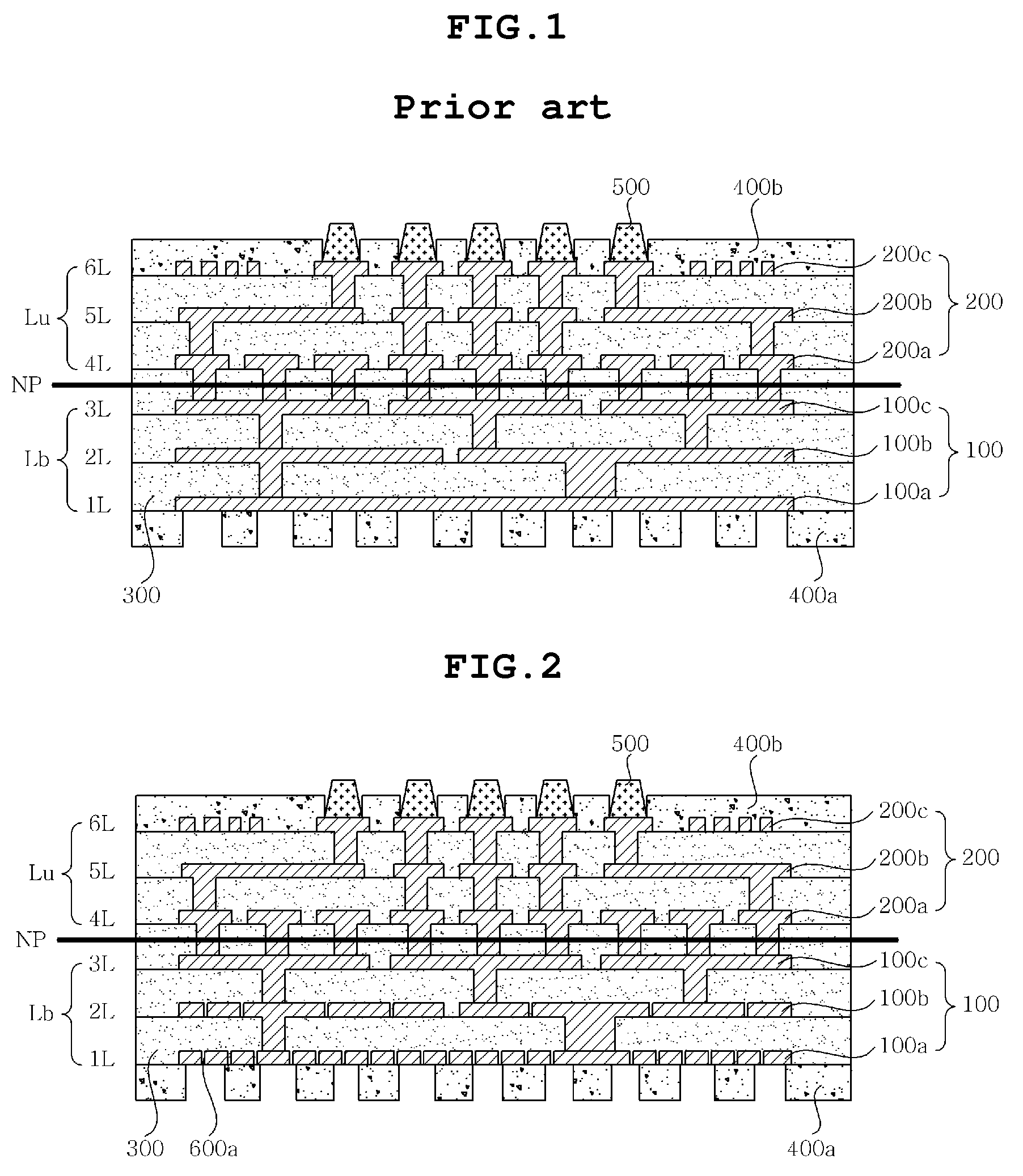
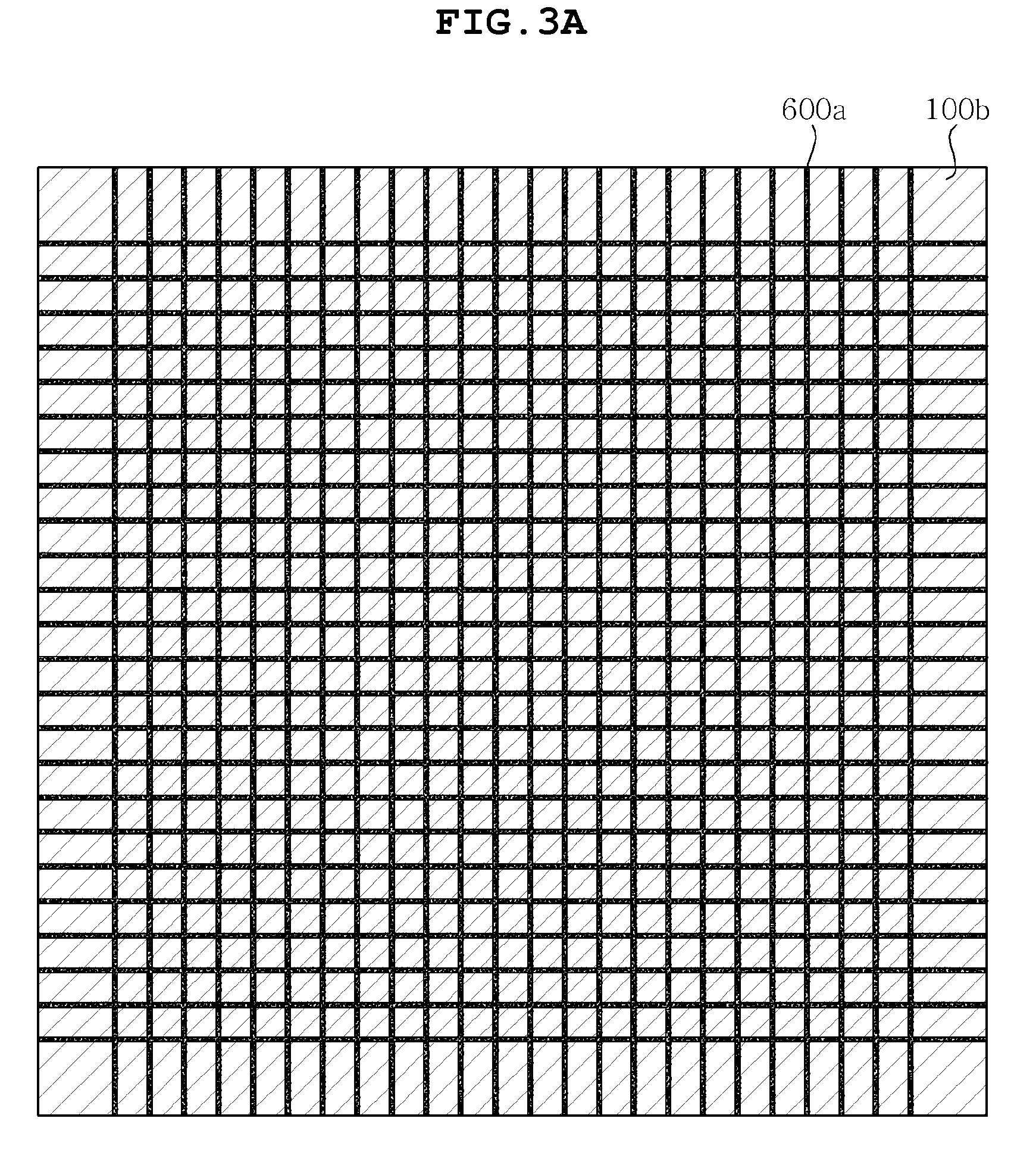
[0035]FIG. 2 is a schematic cross-sectional view showing a package substrate according to the present invention, and FIGS. 3A and 3B are top plan views showing a plating layer formed on a layer, which will be connected to a motherboard, of the package substrate of FIG. 2. Below, the package substrate according to the present embodiment is described with reference to the above drawings.

[0036]As shown in FIGS. 2, 3A and 3B, the package substrate according to the present embodiment is configured such that the plating area of a first plating layer 100 of a layer Lb which will be connected to a motherboard is larger than the plating area of a second plating layer 200 of a layer Lu which will be connected to an electronic part, and open portions 600 are formed on the first plating layer 100.

[0037]Herein, the plating area indicates an area ratio, specifically, a two-dimensional area ratio, between the first plating layer 100 and the second plating layer 200 formed on the insulating layer 3...

second embodiment

[0045]FIGS. 4A and 4B are top plan views showing a plating layer of a layer, which will be connected to a motherboard, of a package substrate according to the present invention.

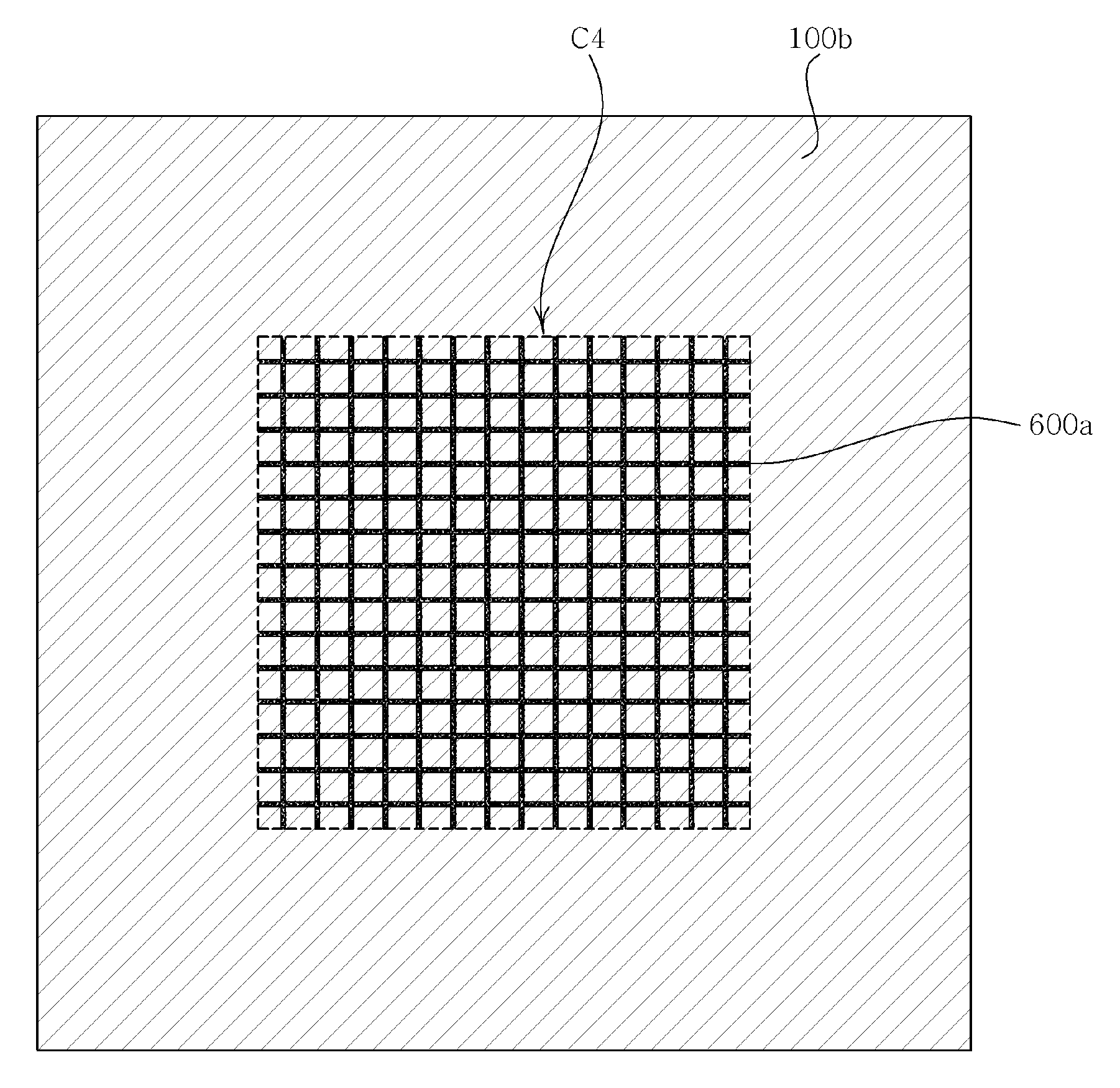
[0046]As shown in FIGS. 4A and 4B, the package substrate according to the present embodiment is configured such that the plating area of a first plating layer 100 formed on a layer, which will be connected to a motherboard and is located on one side of a neutral plane (NP) of the package substrate, of a region corresponding to an electronic part mounting region (C4) of a layer, which will be connected to an electronic part and is located on the other side of the neutral plane (NP) of the package substrate, is larger than the plating area of a second plating layer 200 of the electronic part mounting region (C4), and open portions 600 are formed on the first plating layer 100.

[0047]The present embodiment proposes a structure in which, in consideration of the excessive plating area deviations of the layer which ...


PUM


Abstract

Disclosed is a package substrate, in which the plating area of a first plating layer formed on a layer which is to be connected to a motherboard is larger than the plating area of a second plating layer formed on a layer which is to be connected to an electronic part, and open portions are formed on the first plating layer, thus balancing the plating areas of the plating layers formed on the layers of the package substrate, thereby minimizing warpage of the package substrate due to differing coefficients of thermal expansion.

Description

CROSS REFERENCE TO RELATED APPLICATION[0001]This application claims the benefit of Korean Patent Application No. 10-2009-0090098, filed Sep. 23, 2009, entitled “A package substrate”, which is hereby incorporated by reference in its entirety into this application.BACKGROUND OF THE INVENTION[0002]1. Technical Field[0003]The present invention relates to a package substrate.[0004]2. Description of the Related Art[0005]As an electronic apparatus is being manufactured to have increased performance and a smaller size, the number of terminals of an electronic part such as a semiconductor chip, a die and so on is remarkably increased. In order to easily mount such an electronic part on a motherboard, a package substrate which is adapted for the electrical connection between the electronic part and the motherboard is also made thinner.[0006]Accordingly, a coreless structure which improves signal transmission properties and enables the thickness to be reduced by removing a core substrate is ma...

Claims


Application Information

Patent Timeline
Patent Type & Authority Applications(United States)
IPC IPC(8): H05K1/00
CPCH01L23/49822H01L23/49838H05K1/0224H05K1/0271H05K1/141H05K3/4682H01L2924/0002H05K2201/049H05K2201/09136H05K2201/09681H01L2924/00H05K1/02H05K3/46
Inventor KIM, JIN HOLEE, SEOK KYULEE, JAE JOONJEONG, SUNG WON
Owner SAMSUNG ELECTRO MECHANICS CO LTD
Why Eureka
Try Eureka