Semiconductor circuit

a technology of semiconductor and circuit, applied in the direction of pulse automatic control, pulse technique, electronic switching, etc., can solve the problems of imposing a limit on the ability to remove the error pulse with the phase difference, unintended on/off pulse, and complex total circuit, so as to prevent a malfunction and simple circuit configuration

Active Publication Date: 2011-03-31
MITSUBISHI ELECTRIC CORP
View PDF7 Cites 24 Cited by
  • Summary
  • Abstract
  • Description
  • Claims
  • Application Information

AI Technical Summary

Benefits of technology

[0012]The present invention is directed to overcome the above problem, and an object thereof is to provide a semiconductor circui...

Problems solved by technology

This causes in some cases an unintended ON/OFF pulse (error pulse).
However, because of variation in logic threshold values and/or load resistances within the level shift circuit, and because of the influence of wiring impedance, the error pulses—which would normally occur simultaneously on both ON and OFF pulse sections in the level shift circuit—are in some situations generated with some phase difference.
For that reason, the threshold value of the masking NOT circuit cannot be made much smaller because of area constrai...

Method used


Image

  • Semiconductor circuit
  • Semiconductor circuit
  • Semiconductor circuit

Examples


embodiment 1

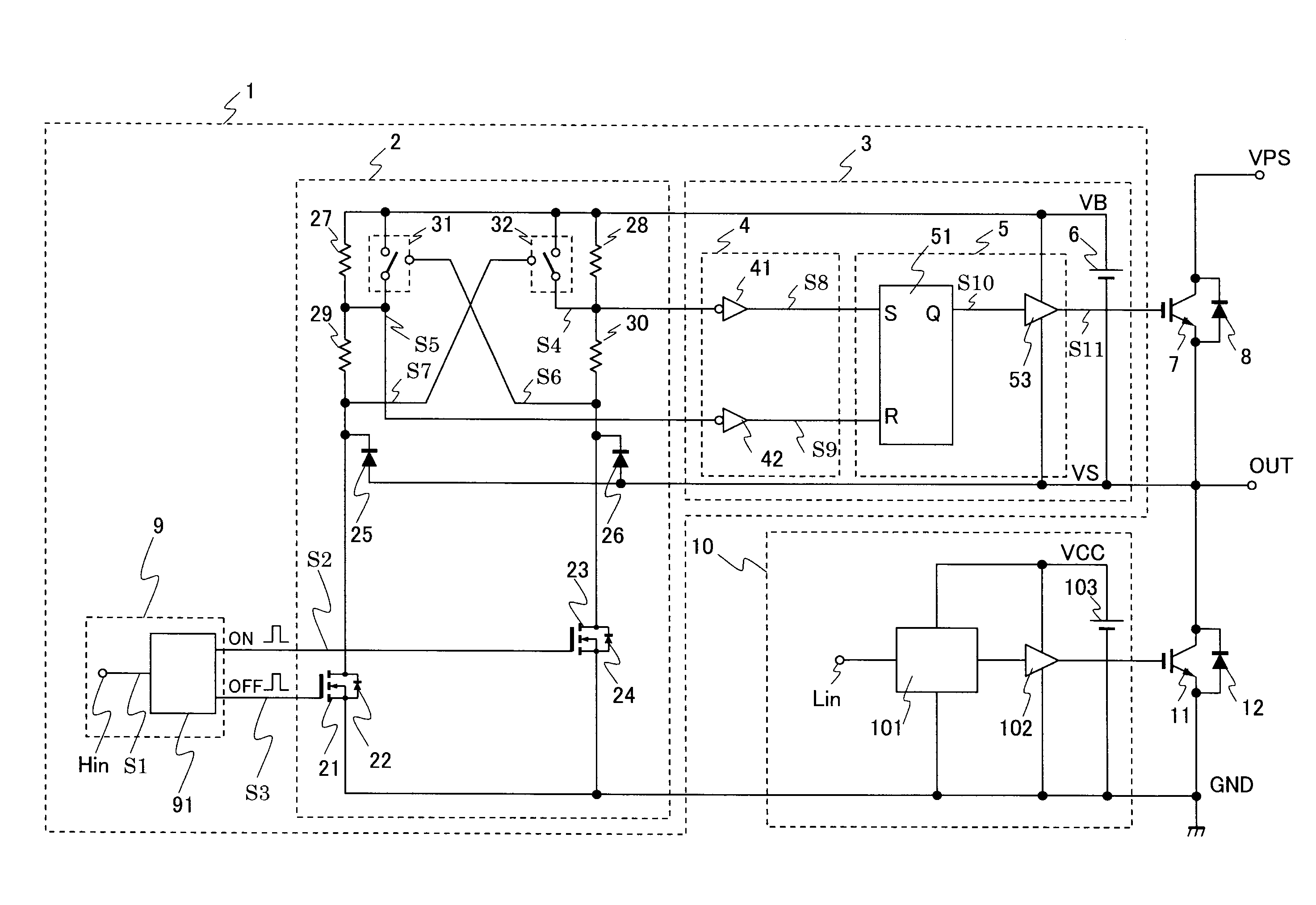
[0021]FIG. 1 shows an embodiment of a semiconductor circuit according to the present invention. Referring to FIG. 1, semiconductor switching devices 7 and 11, such as IGBTs, are connected in series between a main power source potential GND acting as a first potential or the common potential, and a main power source potential VPS of a high potential, which configures a half-bridge inverter circuit. In addition, flyback (or freewheeling) diodes 8 and 12 are connected in inverse parallel with the semiconductor switching devices 7 and 11, respectively, and a load, not shown, is to be connected to a junction—i.e., a terminal OUT—between the semiconductor switching devices 7 and 11.

[0022]Referring to FIG. 1, the semiconductor switching device 7 is called a high potential side switching device because it performs switching operation between a potential at the terminal OUT—the second potential—serving as a reference potential and the main power source VPS of the high potential.

[0023]Further...

embodiment 2

[0059]FIG. 3 shows a semiconductor circuit according to Embodiment 2 of the present invention. Components and signals that are the same as those in Embodiment 1 hereinafter bear the same reference numerals, and their description is not provided.

[0060]In the present embodiment, analog switches 33 and 34 are employed as a specific example of the switch serving as the short circuit device described in Embodiment 1. This enables speedy and accurate control of the short circuit and open circuit.

embodiment 3

[0061]FIG. 4 shows a semiconductor circuit according to Embodiment 3 of the present invention. In the present embodiment, Pch MOS transistors 35 and 36 are used as a specific example of the switch serving as the short circuit device described in Embodiment 1. The use of the Pch MOS transistors configurable by a standard CMOS process enables prevention of an increase in chip size of the semiconductor circuit. Further, since the threshold value of the Pch MOS transistor is about one volt in a typical example, it is possible to easily implement an embodiment circuit, described to be preferable in Embodiment 1, in which the logic threshold values of the short circuit devices are set to be smaller than those of the first and second inverse logic devices 41 and 42.


PUM


Abstract

A semiconductor circuit is provided in which no error signal is generated even when the circuit is exposed to a transient voltage noise that occurs with a transition from a first state indicating a conduction of a high-potential side switching device to a second state indicating a non-conduction of the high potential side switching device, or vice versa. A high potential switching device drive circuit 1 includes short circuit devices 31 and 32 that are controlled by the second level shifted signals S6 and S7 simultaneously generated across the second load resistances 30 and 29, respectively, to thereby serving to prevent a signal from being generated at one of the output sections where the other one of the first level shifted signals S4 and S5 is to be generated, when either one of the first shifted signals S4 and S5 in level shift circuit ON and OFF sections is generated across first load resistance 28 or 27 in a level shift circuit 2.

Description

FIELD OF THE INVENTION[0001]The present invention relates to semiconductor circuits, and particularly to a switching device drive circuit for driving and controlling a semiconductor switching device in which a potential different from a common potential serves as a reference potential.BACKGROUND OF THE INVENTION[0002]In recent years in an application circuit such as a PWM inverter, a synchronous commutation down-converter, and a class-D amplifier, a level shift circuit, by means of a high-voltage integrated circuit, has been used as a circuit for driving a high potential side switching device in two switching devices connected in series between high and low potentials.[0003]A level shift circuit of this kind has a configuration such that, in order to reduce power consumption, only when signal switching occurs between externally supplied command signals that are used to render a semiconductor switching device on the high potential side conductive or non-conductive, a short ON or OFF ...

Claims


Application Information

Patent Timeline
IPC IPC(8): H03L5/00
CPCH03K17/168
Inventor YAMAMOTO, MASAHIRO
Owner MITSUBISHI ELECTRIC CORP
Why Eureka
Try Eureka