
Plasma-based organic mask removal with silicon fluoride

a technology of silicon fluoride and organic mask, applied in the field of electromechanical manufacturing industry, can solve the problems of preventing a via from being adequately filled with conductive material, and the inability to accurately etch organic masks. to achieve the effect of reducing the damage of low-k dielectrics and reducing the lateral etching of etched dielectric features

Inactive Publication Date: 2011-04-07
APPLIED MATERIALS INC
View PDF9 Cites 25 Cited by
  • Summary
  • Abstract
  • Description
  • Claims
  • Application Information

AI Technical Summary

Benefits of technology

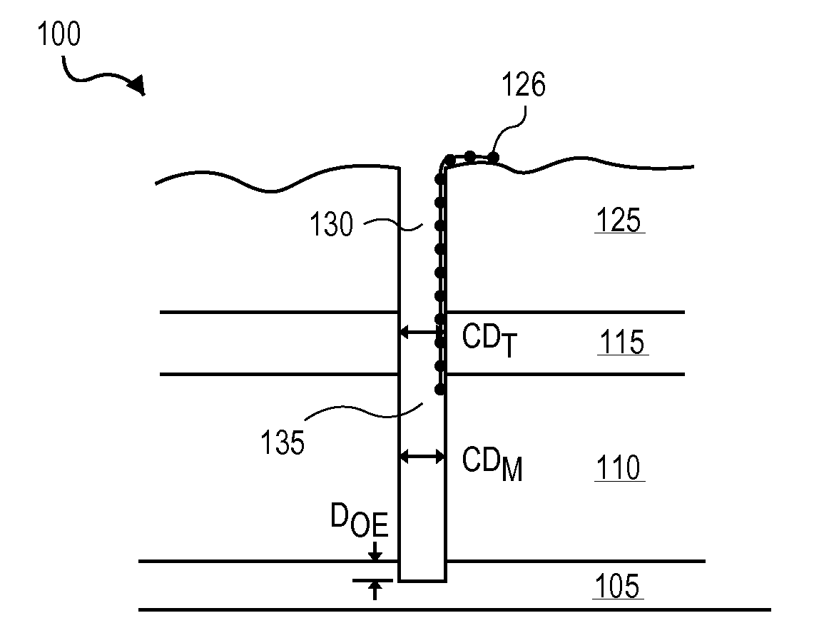
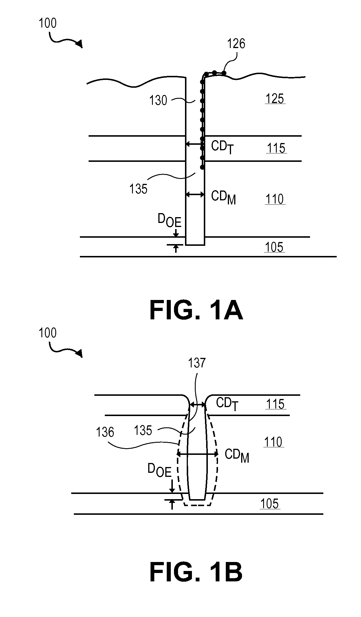
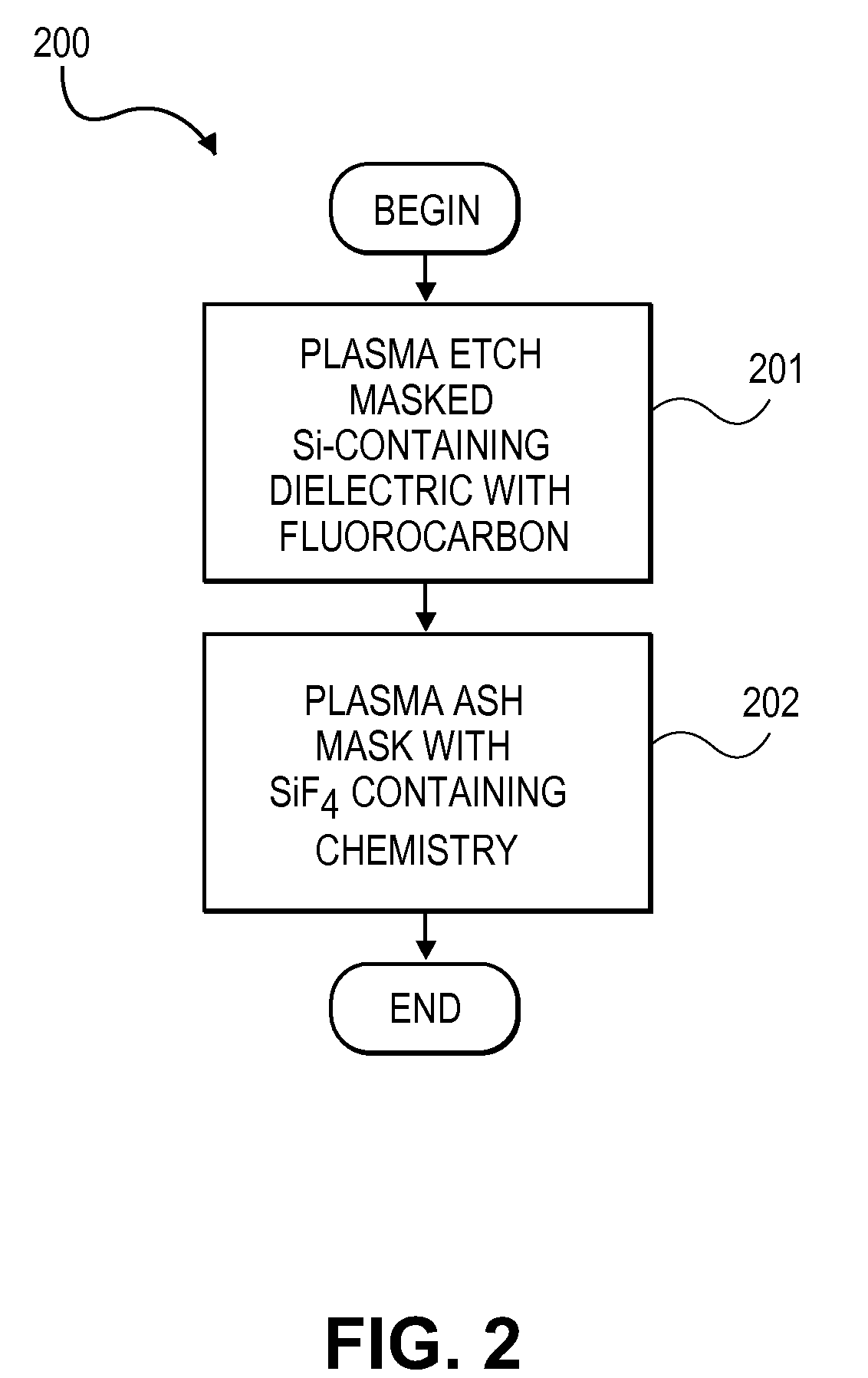
[0008]In a first embodiment, a substrate including an etched dielectric film disposed under an organic mask is provided to a plasma etch chamber. With a fluorocarbon etch product disposed on one or more of the plasma etch chamber, organic mask, or etched dielectric film, the etched dielectric film and organic mask is exposed to a plasma of a first etchant gas including silicon tetrafluoride (SiF4). The etched dielectric film and organic mask may be exposed to the plasma of the first etchant gas for a duration sufficient to remove at least a majority of the organic mask thickness remaining over the etched dielectric film. Addition of the SiF4 to the first etchant gas may reduce the lateral etch of the etched dielectric features (e.g., profile bowing) and reduce the damage of low-k dielectrics caused by the plasma etching / ashing process. Addition of the SiF4 to the first etchant gas may reduce over etch and / or undercut of exposed stop / barrier layers.

Problems solved by technology

As feature sizes are reduced, the proportion of dimensional change attributable to the post-etch organic mask removal process becomes an ever more significant limitation.
Via profile bowing is particularly problematic with low-k (e.g., dielectric constants below about 3.0) and ultra-low-k (e.g., dielectric constants below about 2.5) materials because of their porous nature and mechanical fragility.
Accelerated etch rates of such low-k / ultra low-k materials may lead to undercutting of a dielectric etch stack, which may prevent a via from being adequately filled with conductive material.
The release of fluorocarbons during the post-etch plasma-based organic mask removal process may also deleteriously etch / undercut BEOL hard masks (e.g., non-carbonaceous masks), stop layers, or diffusion barriers exposed during the BEOL dielectric etch.

Method used


Image

  • Plasma-based organic mask removal with silicon fluoride
  • Plasma-based organic mask removal with silicon fluoride
  • Plasma-based organic mask removal with silicon fluoride

Examples


Embodiment Construction

[0016]In the following description, numerous specific details are set forth to provide a thorough understanding of the present invention. It will be apparent to one skilled in the art that the present invention may be practiced without these specific details. In other instances, well-known features, such as specific lithographic patterning and etching techniques, are not described in detail in order to not unnecessarily obscure the present invention. Reference throughout this specification to “an embodiment” means that a particular feature, structure, material, or characteristic described in connection with the embodiment is included in at least one embodiment of the invention. Thus, the appearances of the phrase “in an embodiment” in various places throughout this specification are not necessarily referring to the same embodiment of the invention. Furthermore, the particular features, structures, materials, or characteristics may be combined in any suitable manner in one or more em...


PUM


Abstract

Removal of organic mask material from an etched dielectric film with an etchant gas mixture including silicon fluoride (SiF4). In certain embodiments, SiF4 is combined in an etchant gas mixture of molecular nitrogen (N2), carbon dioxide (CO2) to in-situ strip an organic mask material from a porous low-k dielectric film that has been etched to form a damascene interconnect structure with reduced etch profile bowing and reduced ashing damage to the low-k dielectric film.

Description

CROSS-REFERENCE TO RELATED APPLICATIONS[0001]This application is related to PROVISIONAL PATENT APPLICATION 61 / 247,902 filed Oct. 1, 2009, incorporated by reference in its entirety for all purposes.BACKGROUND[0002]1. Field[0003]Embodiments of the present invention relate to the electronics manufacturing industry and more particularly to the process of plasma etching, stripping or ashing of organic masks.[0004]2. Discussion of Related Art[0005]As the feature size of microelectronic devices gets smaller than 100 nm, the critical dimension (CD) requirement of features becomes a more important criterion for stable and repeatable device performance. Allowable CD variation across a substrate has also scaled with the scaling of feature CD. For example, across a 300 mm diameter substrate, some applications may demand a 3-sigma of less than 10 nm for a target CD averaging about 80 nm.[0006]For back end of line (BEOL) etch processes, post-etch organic mask removal processes may enlarge the CD ...

Claims


Application Information

Patent Timeline
IPC IPC(8): H01L23/522H01L21/768
CPCG03F7/427H01L21/02063H01L23/5226H01L21/76808H01L21/7681H01L21/31138H01L2924/0002H01L2924/00
Inventor ZHOU, YIFENGZHOU, QINGJUNWANG, LINGFUNG, NANCYPENDER, JEREMIAH T.
Owner APPLIED MATERIALS INC
Learn More