Driving method of semiconductor device

a driving method and semiconductor technology, applied in static storage, digital storage, instruments, etc., can solve the problems of negative shift to the threshold voltage, ease of discharge where charges are not sufficiently discharged, wrong data reading, etc., and achieve the effect of reducing the defect of wrong data reading

Active Publication Date: 2011-04-07
SEMICON ENERGY LAB CO LTD
View PDF17 Cites 6 Cited by
  • Summary
  • Abstract
  • Description
  • Claims
  • Application Information

AI Technical Summary

Benefits of technology

[0018]By one embodiment of the present invention, it is possible to provide a driving method of a semiconductor device in which defects of reading wrong data are reduced by judging whether a storage state held in a non-volatile memory element is correct or not in the case where accumulation or discharge of electrons is not enough.

Problems solved by technology

In this case, when a potential supplied to each wiring is unstable, charges are not sufficiently discharged from the charge accumulation layer of the non-volatile memory element and it is possible that a defect caused by reading wrong data occurs.
A problem occurring in the ease where charges are not sufficiently discharged from a charge accumulation layer of a non-volatile memory element is described in more detail.
Further, in the case where a potential of each wiring is lower than that in FIG. 6A in the operation of discharging charges from a charge accumulation layer, a negative shift to the threshold voltage by the operation of discharging charges from a charge accumulation layer is not sufficient in some cases.
Further, in the case where a potential of each wiring is lower than that in FIG. 6B in the operation of discharging charges from a charge accumulation layer, a negative shift to the threshold voltage is not sufficient by the operation of discharging charges from a charge accumulation layer in some cases.
The case of FIG. 6C is the most problematic because a reading error is not detected even when wrong data is read out.

Method used


Image

  • Driving method of semiconductor device
  • Driving method of semiconductor device
  • Driving method of semiconductor device

Examples


embodiment 1

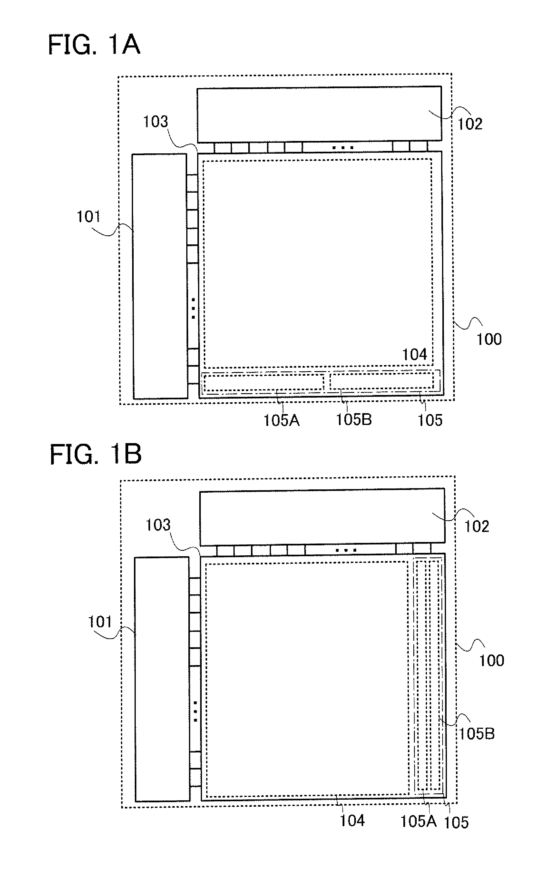
[0035]First, an example of a structure of a memory cell region (also referred to as a memory cell array) and a control circuit (also referred to as a driver circuit) which are included in a semiconductor device is illustrated in FIGS. 1A and 1B. A semiconductor device 100 in FIGS. 1A and 1B includes a row decoder 101, a column decoder 102, and a semiconductor memory circuit 103. The semiconductor memory circuit 103 includes a memory cell region 104 in which memory cells each including a non-volatile memory element are arranged in matrix, and a test region 105.

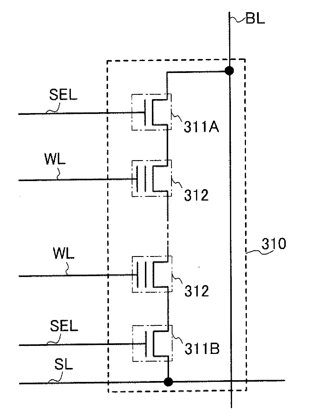
[0036]The test region 105 includes a first region 105A and a second region 105B. Note that FIG. 1A illustrates a structure in which the test region 105 is provided in parallel to the column decoder 102 such that the first region 105A and the second region 10513 in the test region 105 are controlled by one word line and selection line which are extended from the row decoder 101. That is, a memory cell is connected to the first r...

embodiment 2

[0081]In this embodiment, a structure of FIG. 1B will be described with reference to FIG. 8 and FIG. 9. Note that description which overlaps with Embodiment 1 is omitted and the description of Embodiment 1 is employed.

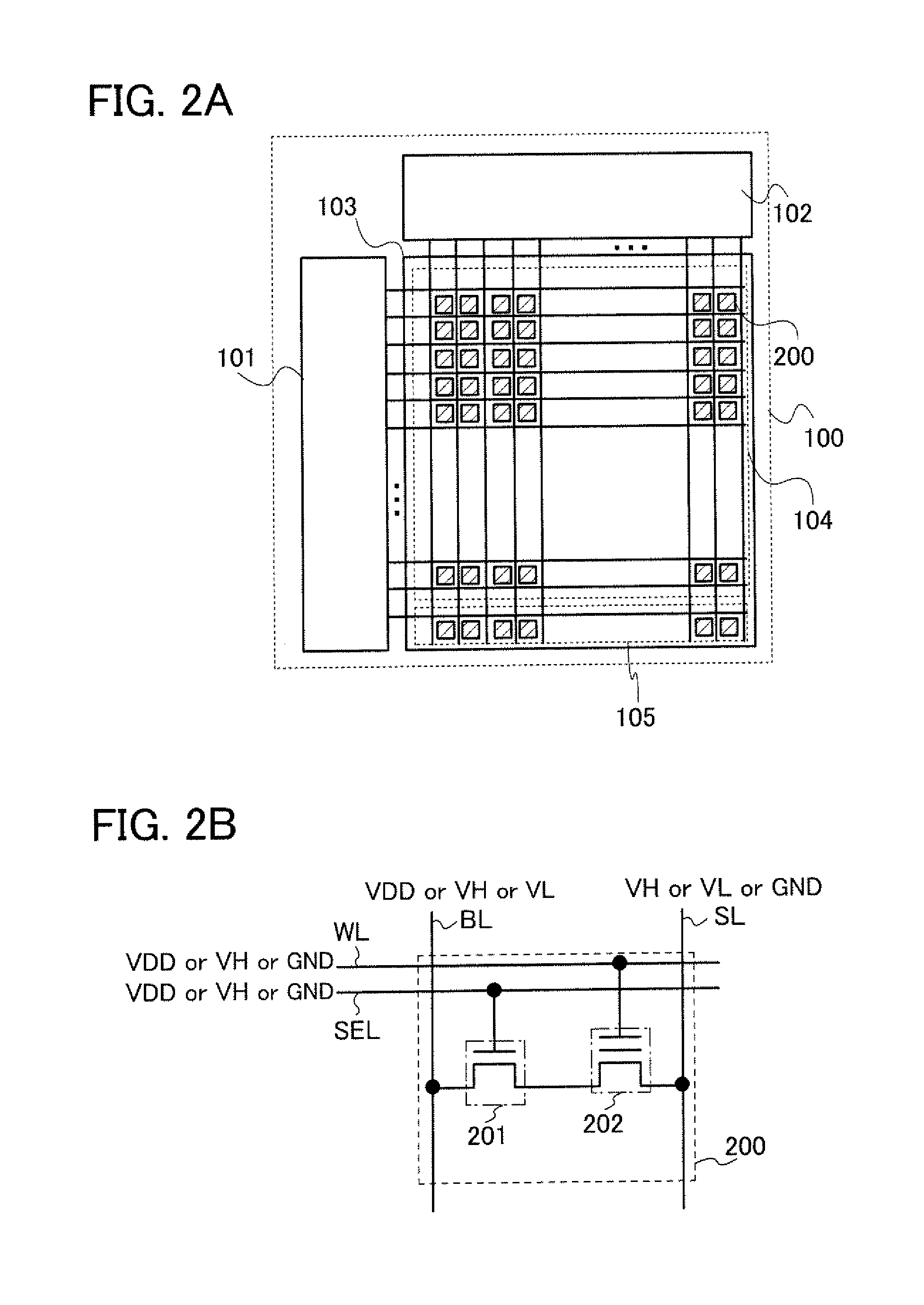
[0082]FIG. 8 specifically illustrates the memory cells in the memory cell region and the test region in FIG. 1B. The semiconductor device 100 illustrated in FIG, 8 includes the row decoder 101, the column decoder 102, and the semiconductor memory circuit 103 including the memory cell region 104 and the test region 105 as in FIG. 1B. The memory cell region 104 and the test region 105 include the memory cells 200 arranged in matrix. As an example, FIG. 8 illustrates a structure in which the memory cells 200 are arranged in a grid pattern.

[0083]Note that the description of the memory cell region 104, a structure of the memory cell 200, and a driving method of the semiconductor device 100 are the same as those in Embodiment 1.

[0084]Note that as illustrated in FIG. 9, the f...

embodiment 3

[0087]In this embodiment, a semiconductor memory device according to one embodiment of the present invention will be described.

[0088]An example of a structure of the semiconductor device described in the above embodiment is illustrated in FIG. 10.

[0089]In addition, FIG. 10 illustrates each signal input and output as well as a block diagram of the semiconductor device described in Embodiment 1. A semiconductor device 1000 illustrated in FIG. 10 includes an interface portion 1001, a boosting circuit 1002, the row decoder 101, the column decoder 102, and the semiconductor memory circuit 103.

[0090]Note that the semiconductor memory circuit 103 includes the memory cell region and the test region as in the above embodiment. To the interface portion 1001, address data (address) of the memory cell region and the test region in the semiconductor memory circuit 103, a writing control signal (WE), and a reading control signal (RE) are input from the outside of the semiconductor device 1000. Fu...


PUM


Abstract

It is an object to reduce defects caused by reading wrong data by judging whether a storage state held in a non-volatile memory element is correct or not in the case where accumulation or discharge of electrons in/from a charge accumulation layer.
A semiconductor memory circuit including a memory cell region and a test region and a control circuit are included in a semiconductor device of the present invention. In the control circuit, a first operation is performed for writing data to a memory cell, and writing a first storage state to a first region or writing a second storage state to a second region. Then, a second operation is performed for reading a first storage state or a second storage state from a first region and a second region. Further, a third operation is performed for reading data from the memory cell. Whether the third operation is correctly performed or not is judged in accordance with whether the first storage state is read from the first region or not or whether the second storage state is read from the second region or not in the second operation.

Description

BACKGROUND OF THE INVENTION[0001]1. Field of the Invention[0002]The present invention relates to a driving method of a semiconductor device. The present invention relates to a driving method of a semiconductor device including a non-volatile memory element in which data can be written and erased.[0003]Note that in this specification, a semiconductor device refers to a device which can function by utilizing semiconductor properties.[0004]2. Description of the Related Art[0005]Non-volatile memory elements are semiconductor elements which can hold data semi-permanently by electrical or physical operation. Non-volatile memory elements can hold a plurality of storage states utilizing the fact that the threshold voltage changes depending on the amount of charge accumulated in charge accumulation layers.[0006]The threshold voltage of a non-volatile memory element is shifted in a positive direction when electrons are accumulated a lot in a charge accumulation layer, and shifted in a negativ...

Claims


Application Information

Patent Timeline
Patent Type & Authority Applications(United States)
IPC IPC(8): G11C16/04
CPCG11C11/5642G11C16/34G11C16/26
Inventor SAITO, TOSHIHIKO
Owner SEMICON ENERGY LAB CO LTD
Why Eureka
Try Eureka