Variable-gain low noise amplifier

a low-noise amplifier and variable-gain technology, applied in the direction of gain control, amplification control details, amplification control device circuits, etc., can solve the problems of deteriorating the linearity of the amplifier, affecting the signal, and sometimes greater interference and noise than the useful signal

Inactive Publication Date: 2011-04-28
SUNPLUS TECH CO LTD
View PDF11 Cites 18 Cited by
  • Summary
  • Abstract
  • Description
  • Claims
  • Application Information

AI Technical Summary

Problems solved by technology

However, in the broadband communication application, the interference and noise are sometimes greater than the useful signal.
If the increase of the noise figure is too obvious, however, the magnitude of the output signal vo fails to provide a sufficient signal-to-noise ratio (SNR), and thus the baseband circuit fails to effectively restore the signal.
The changes of the variable emitter resistors (1Re) 40, however, may deteriorate the linearity of the amplifier.

Method used


Image

  • Variable-gain low noise amplifier
  • Variable-gain low noise amplifier
  • Variable-gain low noise amplifier

Examples


first embodiment

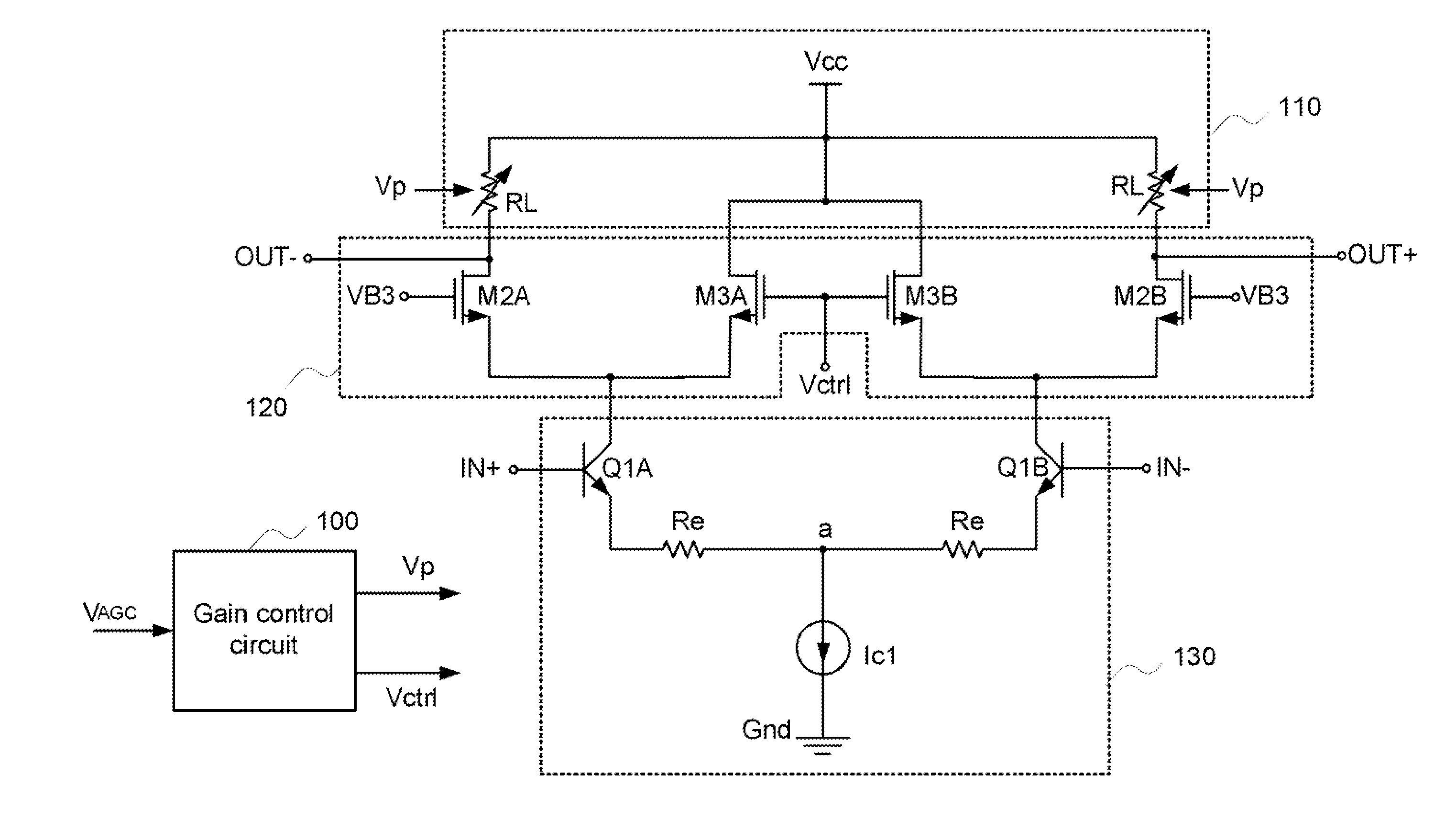
[0031]FIG. 3B is a schematic circuit diagram illustrating a highly linear variable-gain low noise amplifier according to the present invention. The input circuit 130 comprises a first bipolar junction transistor (BJT) Q1A, a second bipolar junction transistor Q1B, two emitter resistors Re and a first current source Ic1. The first bipolar junction transistor Q1A and the second bipolar junction transistor Q1B are connected with each other to define a differential pair. The bases of the first bipolar junction transistor Q1A and the second bipolar junction transistor Q1B are used as the differential signal input terminals (IN+, IN−) of the amplifier. The first terminal of the two emitter resistors Re are respectively connected to the emitters of the first bipolar junction transistor Q1A and the second bipolar junction transistor Q1B. The second terminals of the two emitter resistors Re are collectively connected to a node “a”. The first current source (Ic1) is interconnected between the...

second embodiment

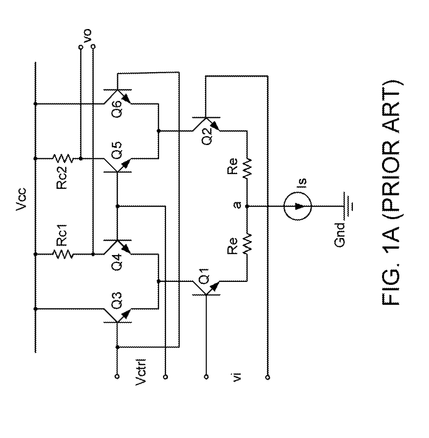
[0037]FIG. 3C is a schematic circuit diagram illustrating a highly linear variable-gain low noise amplifier according to the present invention. In comparison with FIG. 3B, the amplifier of FIG. 3C further comprises a second current source Ic2 and a third current source Ic3. The second current source Ic2 is interconnected between the voltage source Vcc and the collector of the first bipolar junction transistor Q1A. The third current source Ic3 is interconnected between the voltage source Vcc and the collector of the second bipolar junction transistor Q1B. The first current source Ic1, the second current source Ic2 and the third current source Ic3 may provide DC bias voltages to all transistors of the amplifier. As a consequence, the amplifier may be operated at a proper quiescent point. Moreover, the small signal model of the amplifier is not influenced by the first current source Ic1, the second current source Ic2 and the third current source Ic3.

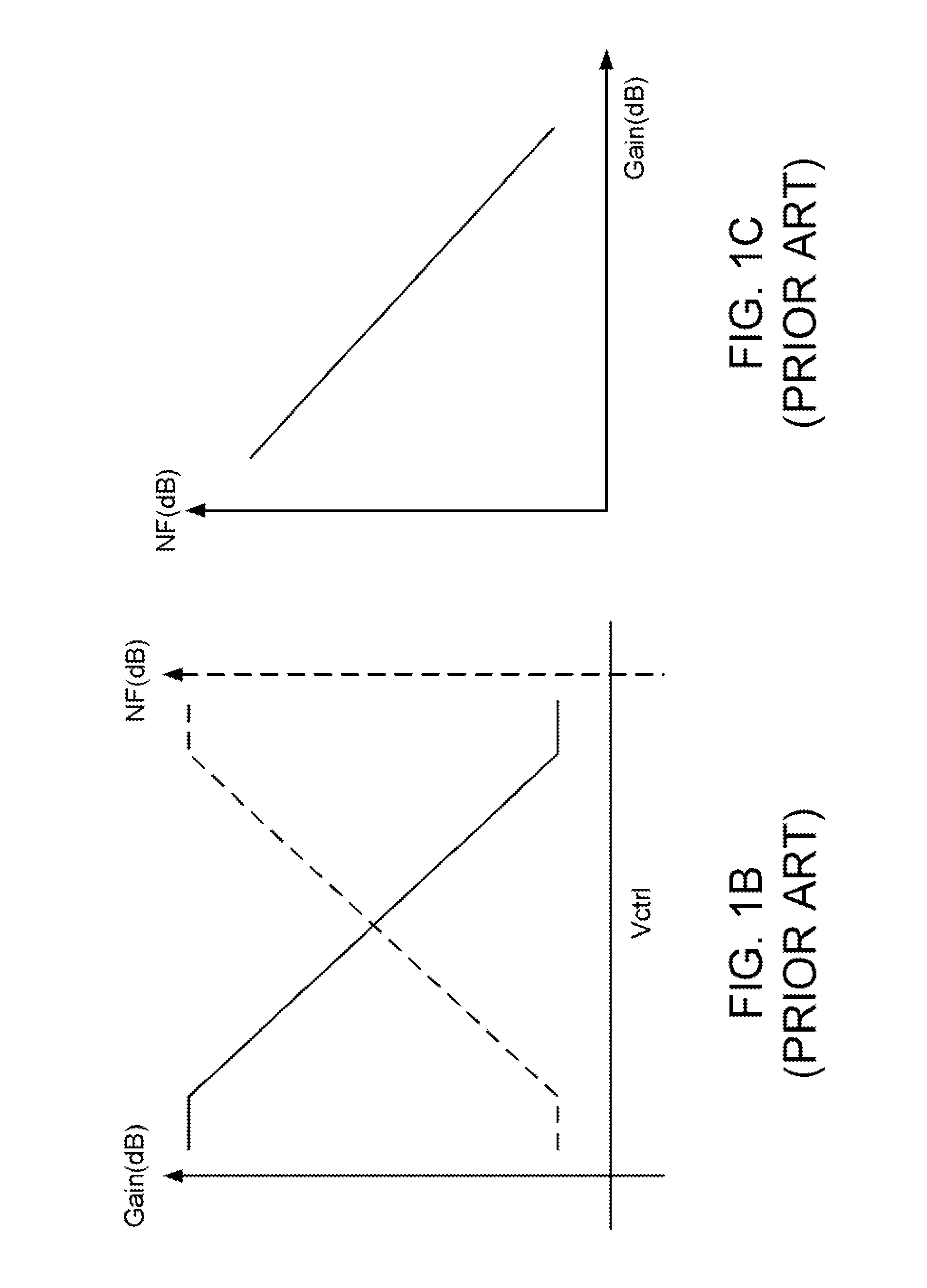
[0038]From FIGS. 3B and 3C, the volt...


PUM


Abstract

A highly linear variable-gain low noise amplifier is a cascode amplifier. The cascode amplifier includes a gain control circuit, a load circuit, a current steering circuit and an input circuit. The gain control circuit is used for receiving a gain adjusting voltage, thereby generating a resistance adjusting signal and a current steering control signal. The load circuit includes plural variable resistors. The resistances of the variable resistors are adjusted according to the resistance adjusting signal. The current steering circuit is connected to the load circuit through plural current paths for adjusting a current ratio between the plural current paths according to the current steering control signal. The current steering circuit has differential signal output terminals. The input circuit is connected to the current steering circuit. The input circuit has differential signal input terminals.

Description

[0001]This application claims the benefit of Taiwan application Serial No. 098135975, filed Oct. 23, 2009, the subject matter of which is incorporated herein by reference.FIELD OF THE INVENTION[0002]The present invention relates to a variable-gain low noise amplifier, and more particularly to a highly linear variable-gain low noise amplifier applied to a TV tuner or other broadband communication systems in order to provide low noise figure at the low gain value.BACKGROUND OF THE INVENTION[0003]In the broadband communication system such as a TV tuner, a highly linear variable-gain low noise amplifier is arranged in upstream of a mixer. Generally, the highly linear variable-gain low noise amplifier is implemented according to a current steering topology.[0004]FIG. 1A is a schematic circuit diagram illustrating a conventional highly linear variable-gain amplifier. This highly linear variable-gain amplifier is disclosed in IEEE J. Solid-State Circuits, vol. 26, pp. 1673-1680, November 1...

Claims


Application Information

Patent Timeline
Patent Type & Authority Applications(United States)
IPC IPC(8): H03F1/22H03F3/45H03G3/30
CPCH03F3/4508H03F3/45286H03F2203/45304H03F2203/45372H03G1/007H03F2203/45394H03F2203/45686H03F2203/45702H03G1/0029H03F2203/45392
Inventor CHAN, WEI-CHIA
Owner SUNPLUS TECH CO LTD
Why Eureka
Try Eureka