

Focusing member and optoelectronic device
- Summary
- Abstract
- Description
- Claims
- Application Information
AI Technical Summary
Benefits of technology
Problems solved by technology
Method used
Image

Examples
first embodiment
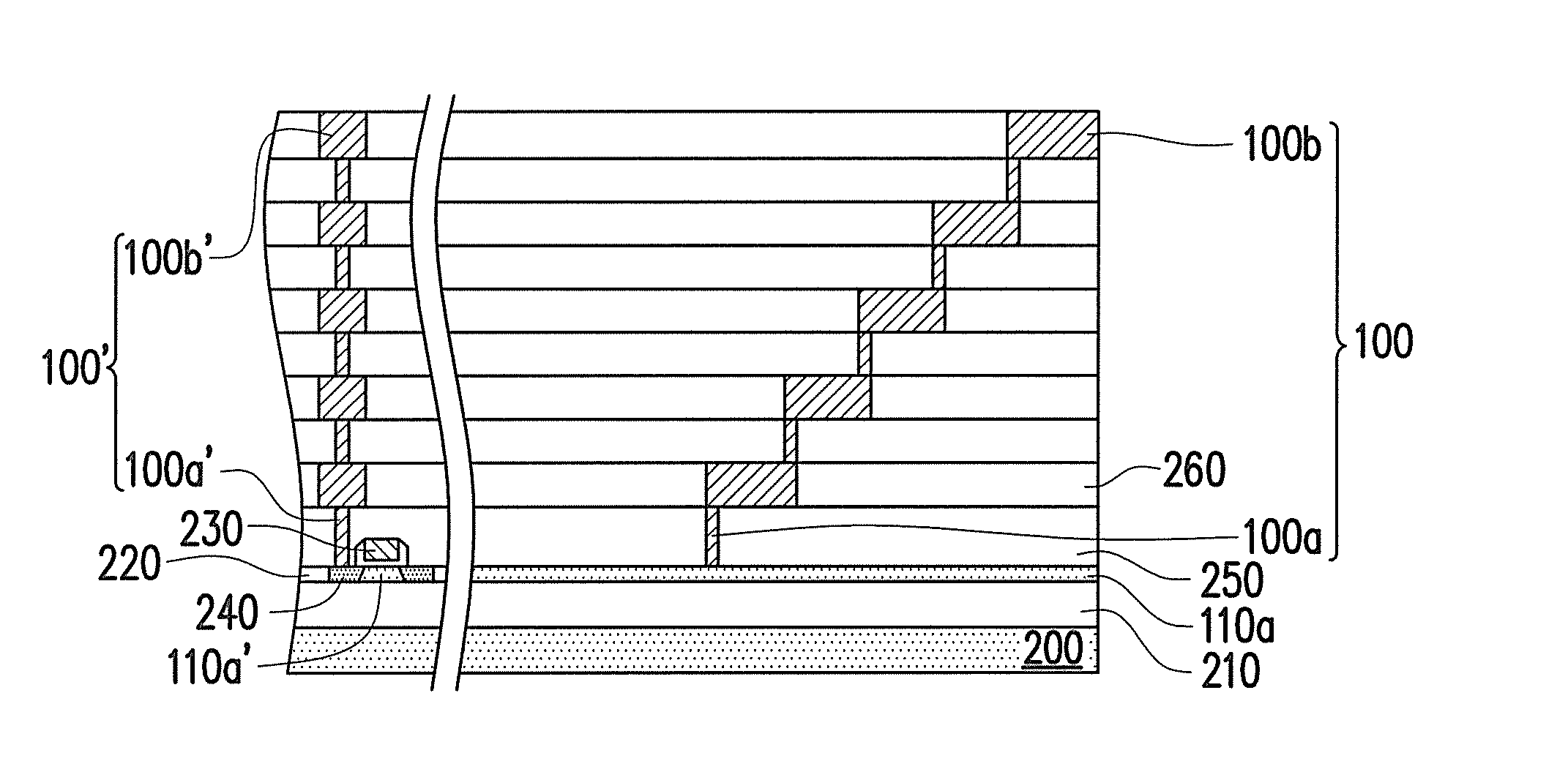
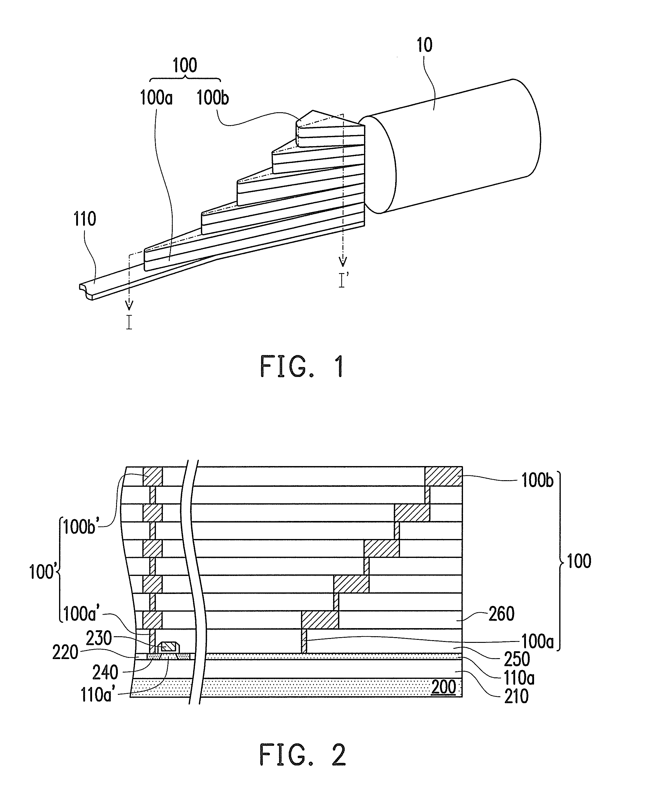
[0023]FIG. 1 illustrates a focusing member, the underlying optical waveguide and the arrangement of the focusing member, the optical waveguide and an optical fiber as an optical signal source, according to the embodiments of this invention. FIG. 2 is a schematic cross-sectional view of an optoelectronic device according to this invention, including a cross-sectional view of the focusing member in FIG. 1 along the line I-I′.
[0024]Referring to FIGS. 1-2, the focusing member 100 is disposed at an edge of the optoelectronic device (FIG. 2), which includes multiple levels of conductive plugs 100a and multiple levels of conductive layers 100b and is disposed over the optical waveguide 110a. The conductive plugs 100a and conductive layers 100b are stacked alternately from top to bottom, and are all bended except the upmost conductive layer 100b. The upper the level of a conductive plug 100a or conductive layer 100b is, the smaller the lateral dimensions of the same is, such that the conduc...
second embodiment
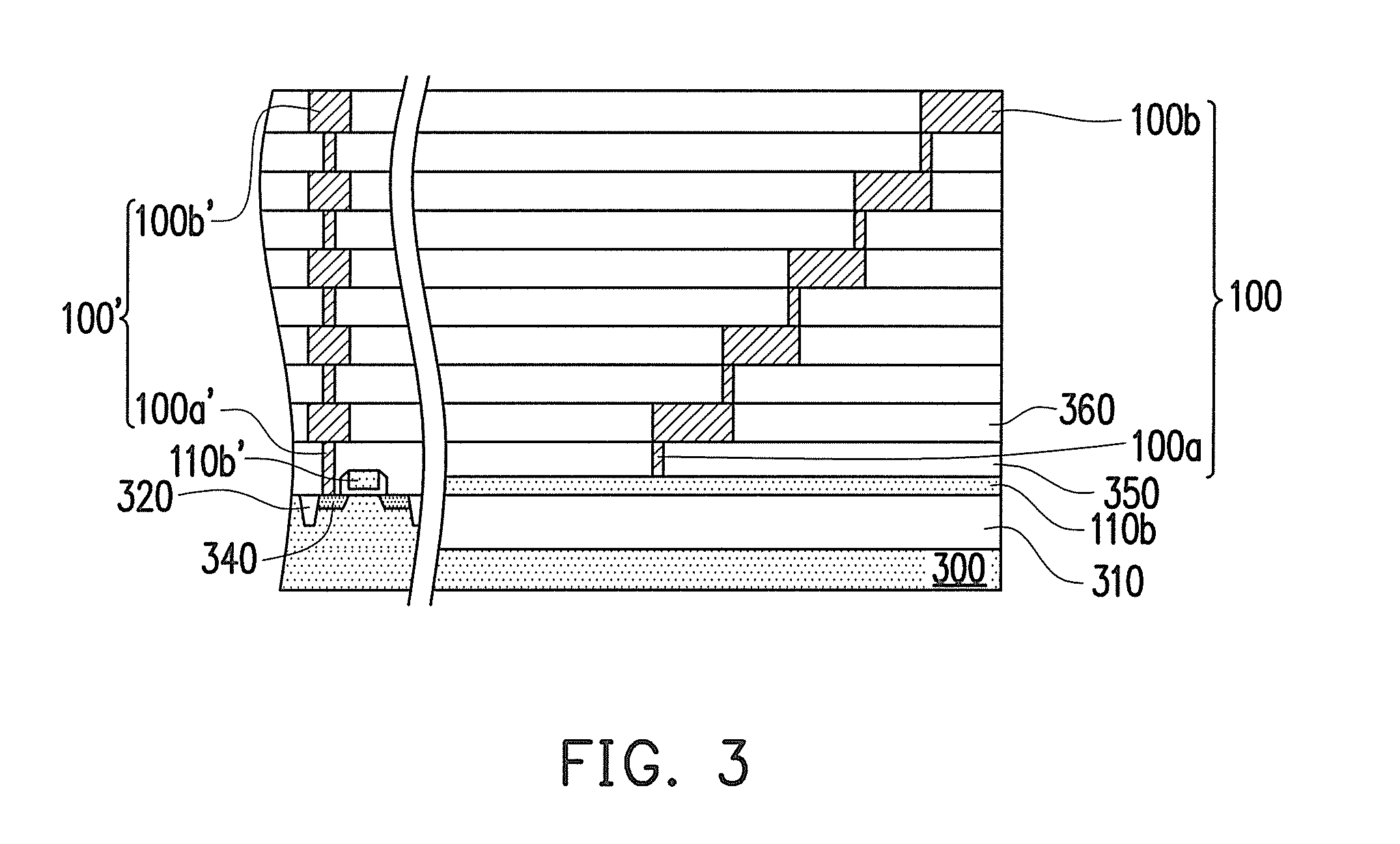
[0029]FIG. 3 is a schematic cross-sectional view of an optoelectronic device according to this invention, including a cross-sectional view of the focusing member in FIG. 1 along the line I-I′.
[0030]In the optoelectronic device of the second embodiment, the focusing member 100 also includes multiple levels of conductive plugs 100a and multiple levels of conductive layers 100b disposed in a dielectric layer that includes an ILD layer 350 and a plurality of IMD layers 360 and covers the optical waveguide 110b. The differences between the second embodiment and the first embodiment include that the substrate is a bulk substrate 300, that the bottom layer under the optical waveguide 110b is a thick insulating layer 310 embedded in the substrate 300, and that the optical waveguide 110b and the gates 110b′ of the CMOS transistors in the integrated circuit are defined from a polysilicon layer formed on the substrate 300. Since the refractive indexes of the insulating layer 310 and the ILD la...
PUM
 Abstract
Description
Claims
Application Information