

Shot blasting material used for silicon substrate surface treatment and method for preparing silicon substrate
- Summary
- Abstract
- Description
- Claims
- Application Information
AI Technical Summary
Benefits of technology
Problems solved by technology
Method used
Image

Examples
exemplary embodiment three
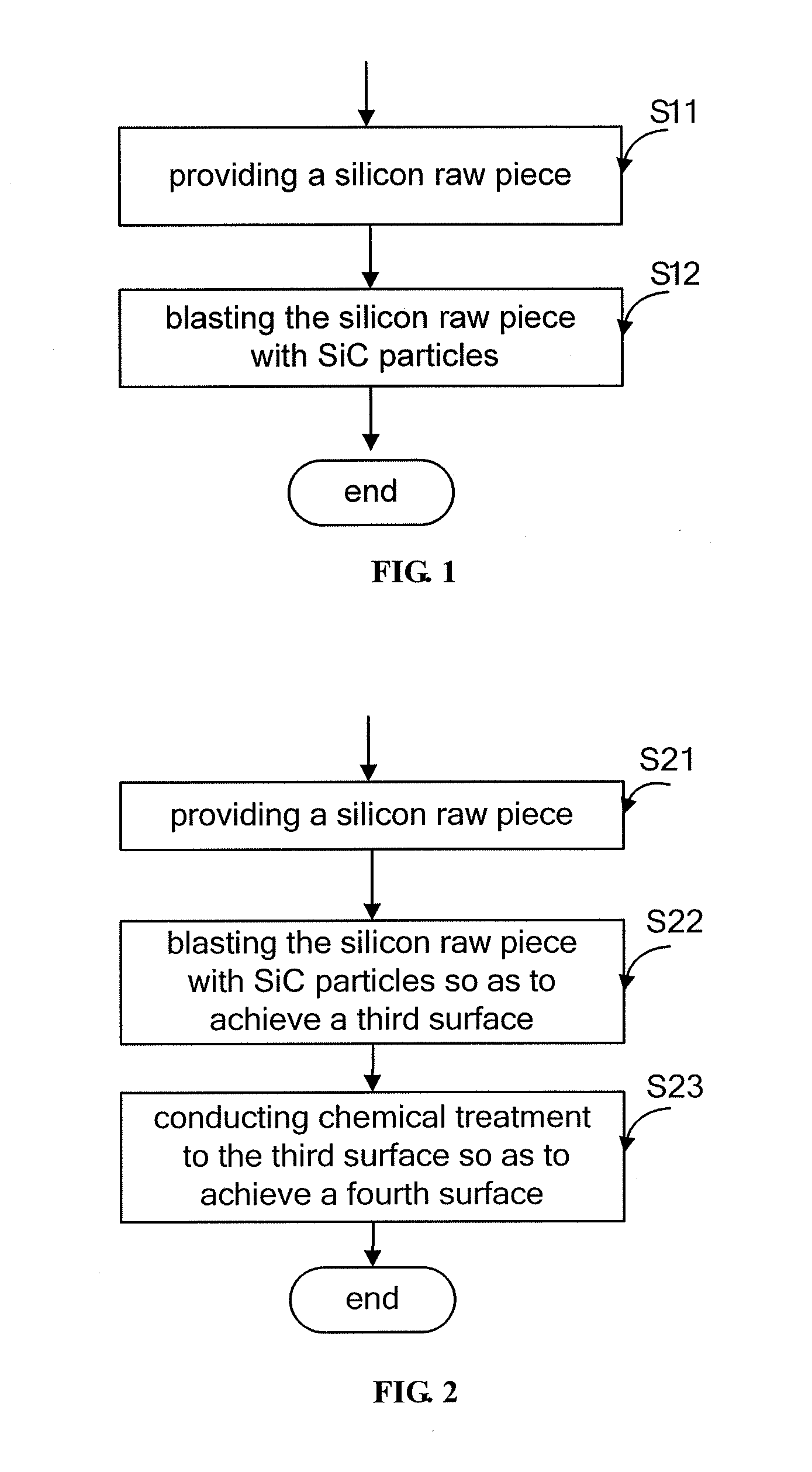
[0170]A blasting material adapted to blast a surface of a silicon substrate is provided. The blasting material may include SiC particles. The blasting material may be used to blast the surface of the silicon substrate in a method described hereinafter. The method may include steps of:
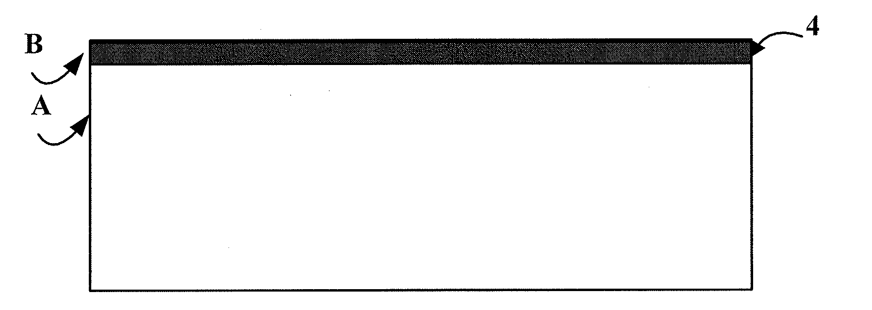
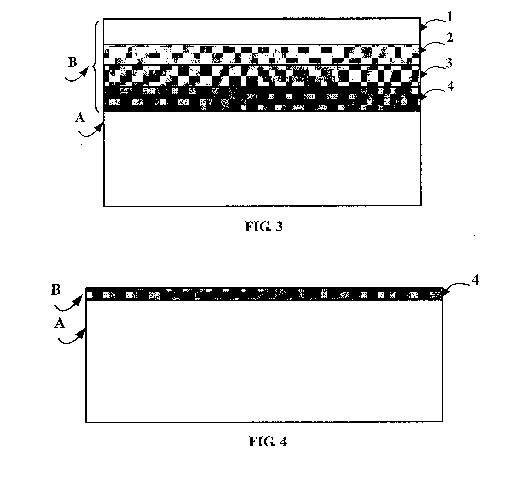
[0171]Step 1: providing a silicon raw piece. The silicon raw piece is produced by applying a crystal ribbon method and includes a first surface and a second surface opposite to the first surface; and the first surface and the second surface substantially have almost no mechanical damage layer. Other physical parameters of the silicon raw piece may include:
[0172]a thickness of 170 μm; and
[0173]a surface reflectivity of 37.59%.
[0174]Step 2: under the action of compressed air, blasting the first surface of the silicon raw piece with the SiC particles.
[0175]1. Physical parameters of the SiC particles in the blasting material may include:
[0176]a median particle diameter of 14.650 μm;
[0177]an average spherici...
PUM
 Abstract
Description
Claims
Application Information