Method for manufacturing vertically structured light emitting diode

Active Publication Date: 2007-04-05
SAMSUNG ELECTRONICS CO LTD
View PDF5 Cites 40 Cited by
  • Summary
  • Abstract
  • Description
  • Claims
  • Application Information

AI Technical Summary

Benefits of technology

[0028] According to the present invention, it is possible to easily perform the chip separation process by selectively wet-etching, breaking or laser-cutting the first plating layer of the device isolation region without an additional dicing process or scribing pr

Problems solved by technology

In addition, since a transparent electrode and the n-electrode are close to each other, the horizontally structured GaN-based LED is vulnerable to electrostatic discharge (ESD).
Otherwise, a complicated process such as scribing and breaking process should be performed.
Therefore, the manufacturing cost is increased and the total process time is delayed resultingly, due to this complicated process.
In addition, in case of using the Si substrate or the GaAs substrate as the conductive substrate 21, the efficiency of heat release is poor and further

Method used


Image

  • Method for manufacturing vertically structured light emitting diode
  • Method for manufacturing vertically structured light emitting diode
  • Method for manufacturing vertically structured light emitting diode

Examples


Example

[0035] Reference will now be made in detail to the preferred embodiments of the present invention, examples of which are illustrated in the accompanying drawings. The invention may, however, be embodied in many different forms and should not be construed as being limited to the embodiments set forth herein; rather, these embodiments are provided so that this disclosure will be thorough and complete, and will fully convey the concept of the invention to those skilled in the art. In the drawings, the shapes and sizes of elements may be exaggerated for clarity, and like reference numerals in the drawings denote like elements.

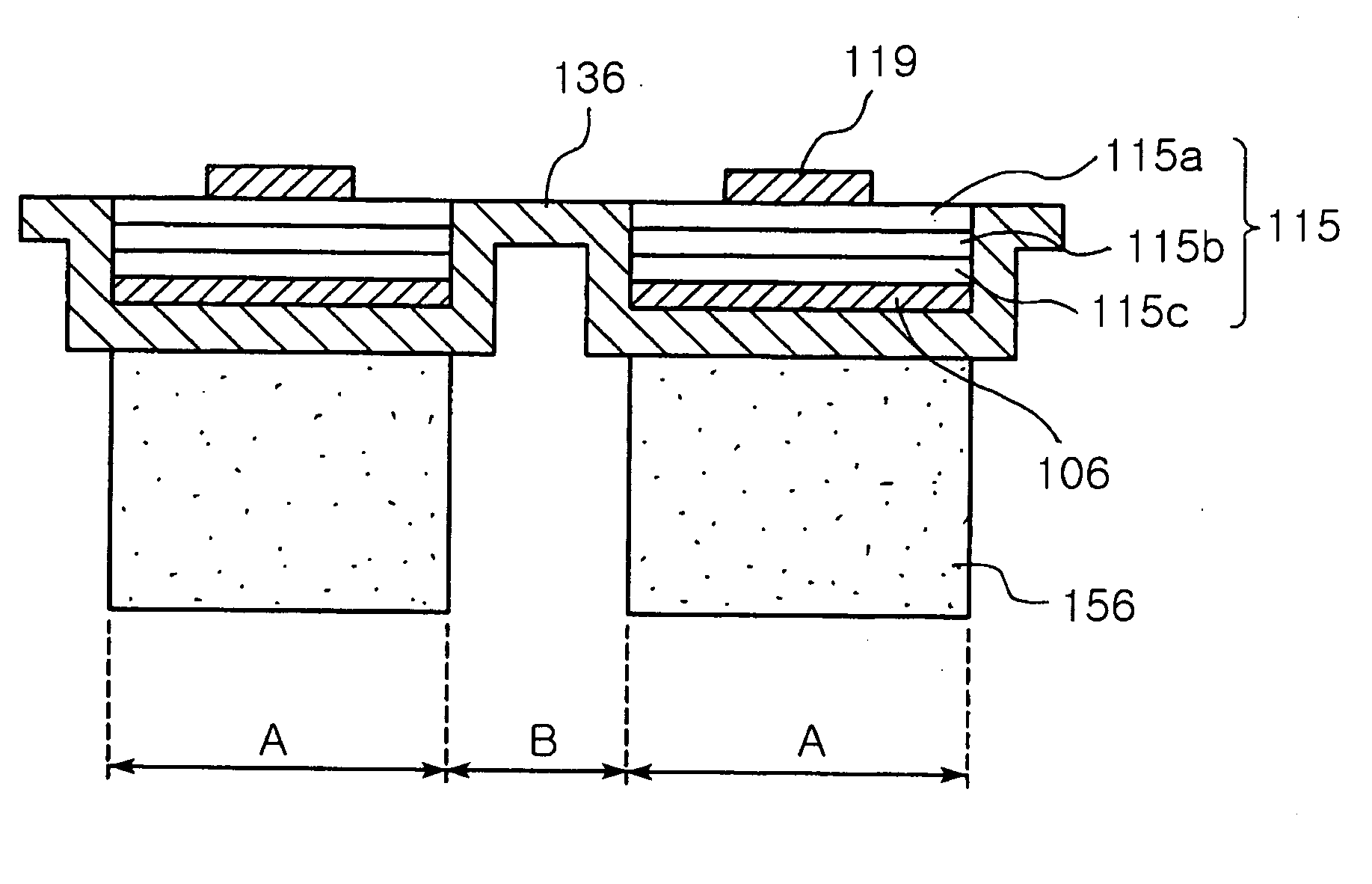
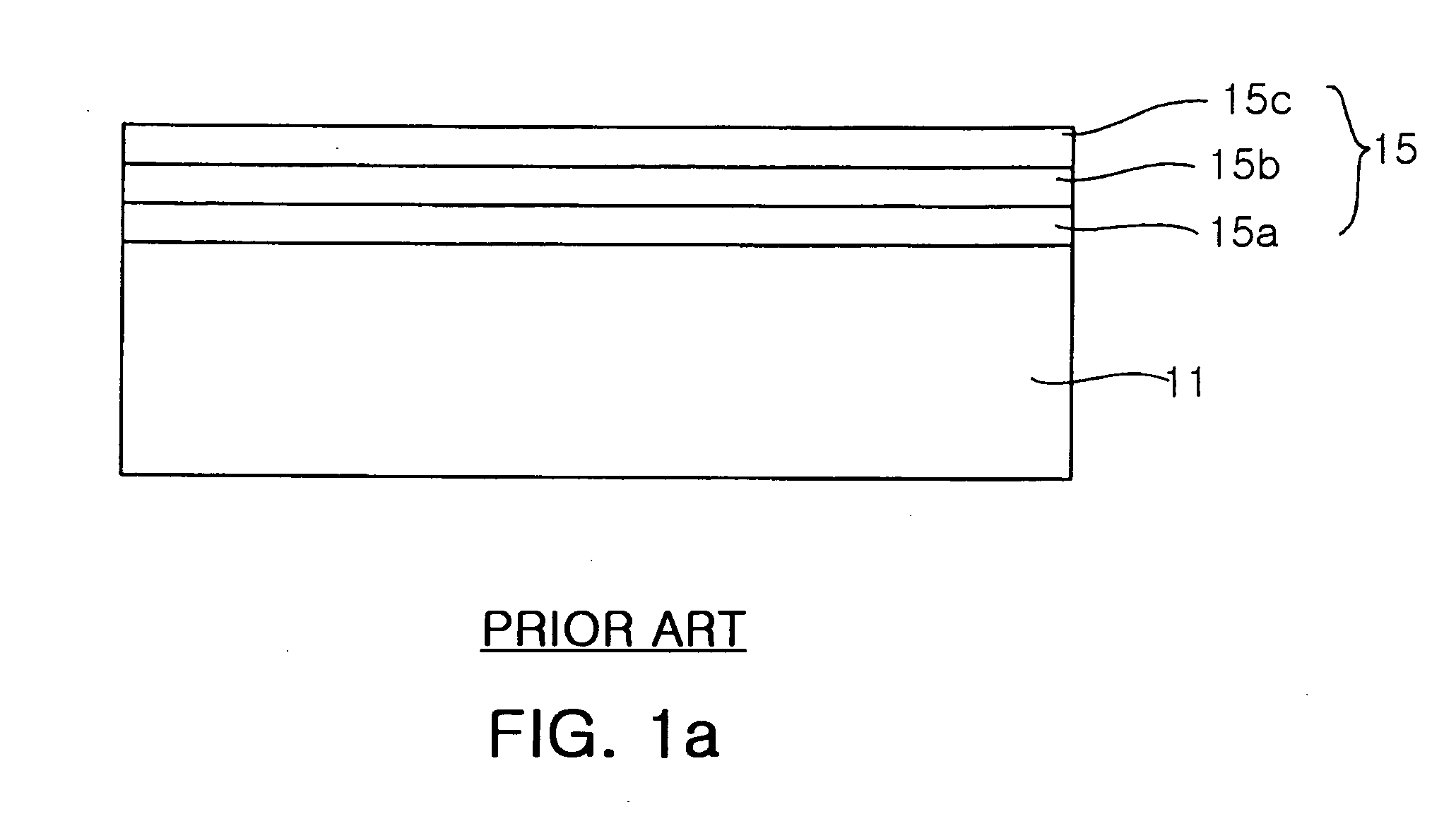
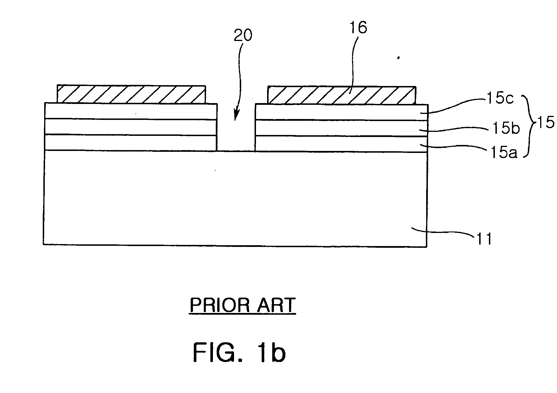
[0036] FIGS. 2 to 11 are cross-sectional views illustrating a method for manufacturing a vertically structured light-emitting diode (LED) according to one embodiment of the present invention. In order to manufacture the LED, a sapphire substrate is used as a growth substrate, and a gallium nitride (GaN)-based semiconductor represented as AlxGayIn1-x-yN (0≦x≦1, 0≦y...


PUM


Abstract

There is provided a method for manufacturing a vertically structured LED capable of performing a chip separation process with ease. In the method, a light-emitting structure is formed on a growth substrate having a plurality of device regions and at least one device isolation region, wherein the light-emitting structure has an n-type clad layer, an active layer and a p-type clad layer which are disposed on the growth substrate in sequence. A p-electrode is formed on the light-emitting structure. Thereafter, a first plating layer is formed on the p-electrode such that it connects the plurality of device isolation regions. A pattern of a second plating layer is formed on the first plating layer of the device region. The growth substrate is removed, and an n-electrode is then formed on the n-type clad layer.

Description

RELATED APPLICATION [0001] The present application is based on, and claims priority from, Korean Application Number 2005-93409, filed Oct. 5, 2005, the disclosure of which is hereby incorporated by reference herein in its entirety. BACKGROUND OF THE INVENTION [0002] 1. Field of the Invention [0003] The present invention relates to a method for manufacturing a semiconductor light emitting device, and more particularly, to a method for manufacturing a vertically structured light emitting diode (LED) capable of easily performing a chip separation process for individual elements. [0004] 2. Description of the Related Art [0005] A gallium nitride (GaN)-based semiconductor, which is represented as AlxGayIn1-x-yN (0≦x≦1, 0≦y≦1, 0≦x+y≦1), is a compound semiconductor material adaptive for light-emitting in ultraviolet region, and is used for a blue or green light emitting diode (LED). The GaN-based LED that is being used up to date is mainly classified into two types, of which one is a horizo...

Claims


Application Information

Patent Timeline
IPC IPC(8): H01L21/00H01L33/32H01L33/44
CPCH01L33/0079H01L33/62H01L2924/0002H01L2924/00H01L33/0093
Inventor HWANG, HAE YEONRYU, YUNG HOSHIM, DA MIAHN, SE HWAN
Owner SAMSUNG ELECTRONICS CO LTD
Why Eureka
Try Eureka