Transistor

a transistor and field effect technology, applied in the field of field effect transistors, can solve the problems of generating channel, flow of leakage current, and unwanted charge buildup in elements, electrodes, or wirings, and achieve the effects of increasing field effect mobility and on-state current, reducing off-state current, and increasing purity

Inactive Publication Date: 2011-05-05
SEMICON ENERGY LAB CO LTD
View PDF99 Cites 42 Cited by
  • Summary
  • Abstract
  • Description
  • Claims
  • Application Information

AI Technical Summary

Benefits of technology

[0016]According to one embodiment of the present invention, the use of an oxide semiconductor in which the hydrogen concentration is reduced and the purity is i

Problems solved by technology

In a display device, there is a problem in that unwanted charge build up in elements, electrodes, or wirings during manufacture or operation.
In the case of, for example, a thin film transistor, such charge build-up might cause generation of a parasitic channel, which leads to flow of leakage current.
Further, in the case of a bottom-gate transistor, charge might build up on a surface of or in a back channel portion in a semi

Method used


Image

  • Transistor
  • Transistor
  • Transistor

Examples


embodiment 1

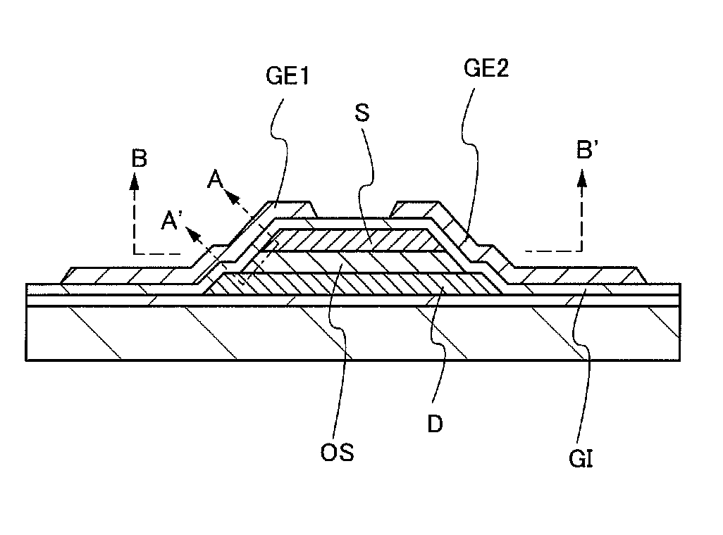
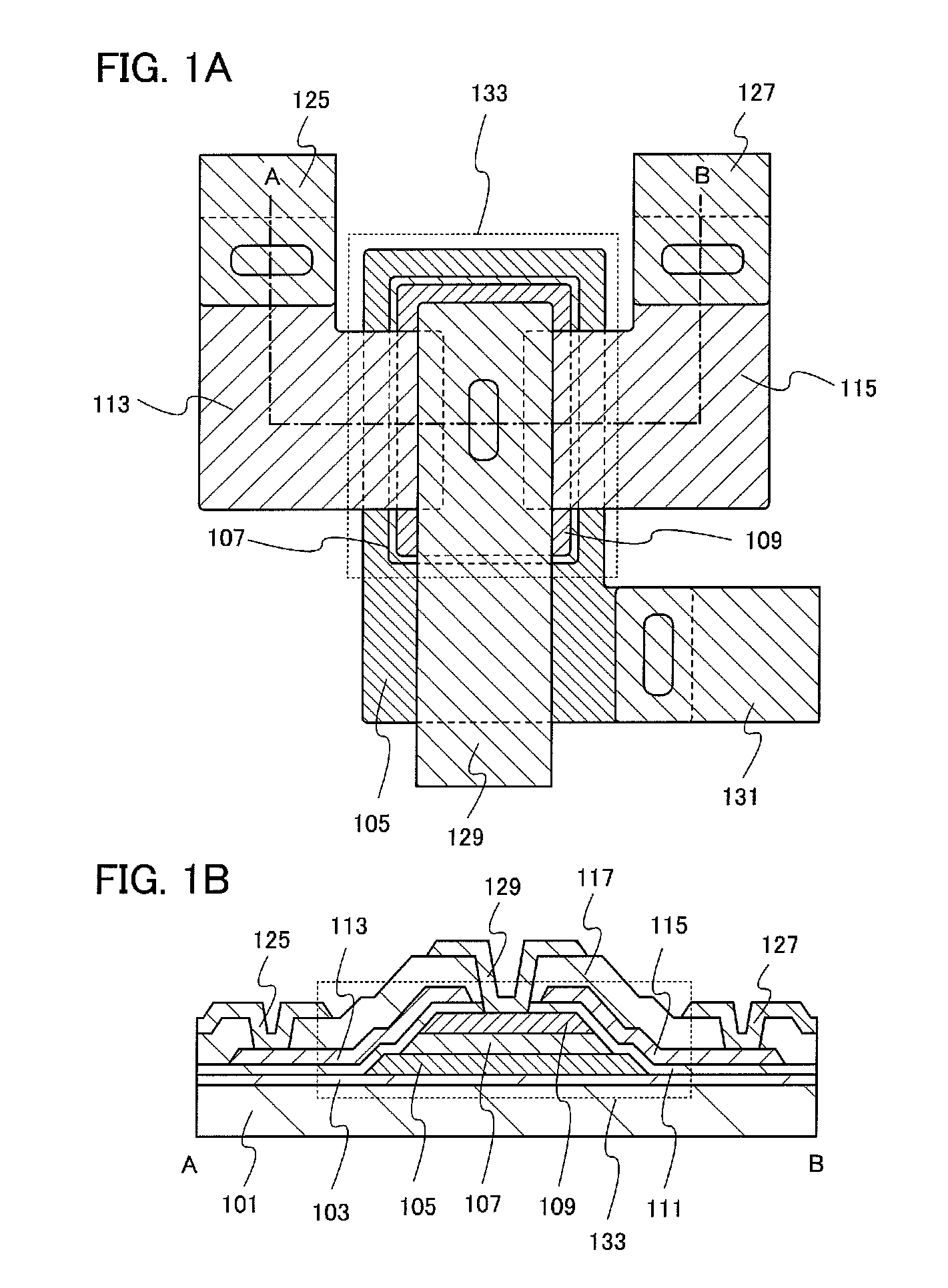
[0038]In this embodiment, a structure of a field effect transistor, for example, a thin film transistor will be described with reference to FIGS. 1A and 1B.

[0039]FIG. 1A is a top view of a thin film transistor 133. FIG. 1B is a cross-sectional view taken along chain line A-B in FIG. 1A.

[0040]As illustrated in FIG. 1B, a first electrode 105, an oxide semiconductor film 107, and a second electrode 109 are stacked over an insulating film 103 formed over a substrate 101. In addition, a gate insulating film 111 is provided so as to cover the first electrode 105, the oxide semiconductor film 107, and the second electrode 109. Third electrodes 113 and 115 are provided over the gate insulating film 111. An insulating film 117 that functions as an interlayer insulating film is provided over the gate insulating film 111 and the third electrodes 113 and 115. Openings are formed in the insulating film 117. A wiring 131 (see FIG. 1A) which is connected to the first electrode 105 through the open...

embodiment 2

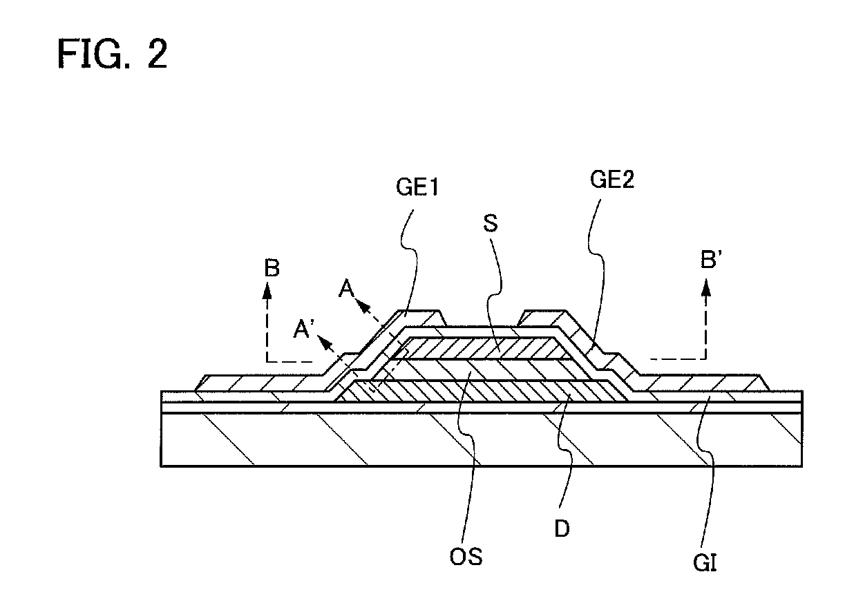
[0072]In this embodiment, a structure of a field effect transistor, for example, a thin film transistor that is different from that of the thin film transistor described in Embodiment 1 will be described with reference to FIGS. 6A and 6B.

[0073]FIG. 6A is a top view of thin film transistors 141 and 143. FIG. 6B is a cross-sectional view taken along chain line A-B in FIG. 6A.

[0074]As illustrated in FIG. 6B, the first electrodes 105 and 106, the oxide semiconductor film 107, and the second electrode 109 are stacked over the insulating film 103 formed over the substrate 101. In addition, the gate insulating film 111 is provided so as to cover the first electrodes 105 and 106, the oxide semiconductor film 107, and the second electrode 109. The third electrodes 113 and 115 are provided over the gate insulating film 111. The insulating film 117 that functions as an interlayer insulating film is provided over the gate insulating film 111 and the third electrodes 113 and 115. Openings are fo...

embodiment 3

[0080]In this embodiment, a field effect transistor, for example, a thin film transistor that is one embodiment of the present invention and is different from the thin film transistors described in the above embodiments will be described.

[0081]FIGS. 7A and 7B illustrate an example of a thin film transistor according to this embodiment.

[0082]The thin film transistor illustrated in FIGS. 7A and 7B has a stacked structure that is similar to that of the thin film transistor described in Embodiment 1. In other words, first electrodes 105A to 105D, the oxide semiconductor film 107, and the second electrode 109 are stacked over the insulating film 103 formed over the substrate 101. In addition, the gate insulating film 111 is provided so as to cover the first electrodes 105A to 105D, the oxide semiconductor film 107, and the second electrode 109. Third electrodes 113A to 113D are provided over the gate insulating film 111. The insulating film 117 that functions as an interlayer insulating ...


PUM


Abstract

To provide a thin film transistor which has high operation speed and in which a large amount of current can flow when the thin film transistor is on and off-state current at the time when the thin film transistor is off is extremely reduced. The thin film transistor is a vertical thin film transistor in which a channel formation region is formed using an oxide semiconductor film in which hydrogen or an OH group contained in the oxide semiconductor is removed so that hydrogen is contained in the oxide semiconductor at a concentration of lower than or equal to 5×10¹⁹/cm3, preferably lower than or equal to 5×10¹⁸/cm3, more preferably lower than or equal to 5×10¹⁷/cm3, and the carrier concentration is lower than or equal to 5×10¹⁴/cm3, preferably lower than or equal to 5×10¹²/cm3.

Description

TECHNICAL FIELD[0001]The present invention relates to field effect transistors, for example, thin film transistors in each of which an oxide semiconductor is used.BACKGROUND ART[0002]A technique for forming a thin film transistor (TFT) by using a semiconductor thin film formed over a substrate having an insulating surface has attracted attention. The thin film transistors have been used in display devices typified by a liquid crystal television. A silicon-based semiconductor material is known as a material for a semiconductor thin film that can be used in thin film transistors. Besides, an oxide semiconductor has attracted attention as another material.[0003]As a material for the oxide semiconductor, zinc oxide or a substance containing zinc oxide is known. Thin film transistors each of which is formed using an amorphous oxide (an oxide semiconductor) having an electron carrier concentration of lower than 1018 / cm3 are disclosed in Patent Documents 1 to 3.REFERENCE[0004][Patent Docum...

Claims


Application Information

Patent Timeline
IPC IPC(8): H01L29/12
CPCH01L27/1225H01L29/78606H01L29/78642H01L29/78693H01L29/7869H01L29/78696H01L29/78648H01L29/06
Inventor YAMAZAKI, SHUNPEI
Owner SEMICON ENERGY LAB CO LTD
Why Eureka
Try Eureka